Datasheet 搜索 > 电压基准芯片 > ADI(亚德诺) > AD581TH 数据手册 > AD581TH 产品设计参考手册 1/13 页

¥ 114.223
AD581TH 产品设计参考手册 - ADI(亚德诺)
制造商:
ADI(亚德诺)
分类:
电压基准芯片
封装:
TO-5-3
描述:
10V,Analog Devices### 电压参考,Analog Devices精密固定和可调电压参考 IC 利用串联、并联或串联/并联拓扑,并提供通孔和表面安装封装。 电压参考的初始准确度为 ±0.02 至 ±2%。
Pictures:
3D模型
符号图
焊盘图
引脚图
产品图
页面导航:
导航目录
AD581TH数据手册
Page:
of 13 Go
若手册格式错乱,请下载阅览PDF原文件

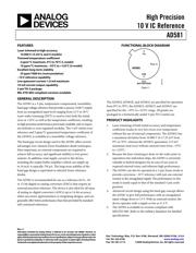
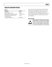
High Precision
10 V IC Reference
AD581
Rev. C
Information furnished by Analog Devices is believed to be accurate and reliable. However, no
responsibility is assumed by Analog Devices for its use, nor for any infringements of patents or other
rights of third parties that may result from its use. Specifications subject to change without notice. No
license is granted by implication or otherwise under any patent or patent rights of Analog Devices.
Trademarks and registered trademarks are the property of their respective owners.
One Technology Way, P.O. Box 9106, Norwood, MA 02062-9106, U.S.A.
Tel: 781.329.4700 www.analog.com
Fax: 781.461.3113 ©2009 Analog Devices, Inc. All rights reserved.
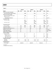
FEATURES
Laser trimmed to high accuracy
10.000 V ±5 mV (L and U models)
Trimmed temperature coefficient
5 ppm/°C maximum, 0°C to 70°C (L model)
10 ppm/°C maximum, −55°C to +125°C (U model)
Excellent long-term stability
25 ppm/1000 hrs (noncumulative)
−10 V reference capability
Low quiescent current: 1.0 mA maximum
10 mA current output capability
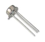
3-pin TO-5 package
MIL-STD-883 compliant versions available
FUNCTIONAL BLOCK DIAGRAM
TO-5
BOTTOM VIEW
+V
S
V
OUT
GND
AD581
08014-001
Figure 1.
GENERAL DESCRIPTION
The AD581 is a 3-pin, temperature compensated, monolithic,
band gap voltage reference that provides a precise 10.00 V output
from an unregulated input level ranging from 12 V to 30 V.
Laser wafer trimming (LWT) is used to trim both the initial
error at +25°C as well as the temperature coefficient, resulting
in high precision performance previously available only in expen-
sive hybrids or oven regulated modules. The 5 mV initial error
tolerance and 5 ppm/°C guaranteed temperature coefficient of
the AD581L is available in a monolithic voltage reference.
The band gap circuit design used in the AD581 offers several
advantages over classical Zener breakdown diode techniques.
Most important, no external components are required to
achieve full accuracy and significant stability to low power
systems. In addition, total supply current to the device,
including the output buffer amplifier (which can supply up
to 10 mA) is typically 750 A. The long-term stability of the
band gap design is equivalent to selected Zener reference
diodes.
The AD581 is recommended for use as a reference for 8-, 10-
or 12-bit digital-to-analog converters (DACs) that require an
external precision reference. The device is also ideal for all types
of analog-to-digital converters (ADCs) up to 14-bit accuracy,
either successive approximation or integrating designs, and can
generally offer better performance than that provided by standard
self-contained references.
The AD581J, AD581K, and AD581L are specified for operation
from 0°C to 70°C; the AD581S, AD581T, and AD581U are
specified for the −55°C to +125°C range. All grades are
packaged in a hermetically sealed 3-pin TO-5 metal can.
PRODUCT HIGHLIGHTS
1. Laser trimming of both initial accuracy and temperature
coefficient results in very low errors over temperature
without the use of external components. The AD581L has
a maximum deviation from 10.000 V of ±7.25 mV from
0°C to 70°C, whereas the AD581U guarantees ±15 mV
maximum total error without external trims from −55°C
to +125°C.
2. Because the laser trimming is done on the wafer prior to
separation into individual chips, the AD581 is extremely
valuable to hybrid designers for its ease of use, lack of
required external trims, and inherent high performance.
3. The AD581 can also be operated in a 2-pin Zener mode to
provide a precision −10 V reference with just one external
resistor to the unregulated supply. The performance in this
mode is nearly equal to that of the standard 3-pin confi-
guration.
4. Advanced circuit design using the band gap concept allows
the AD581 to give full performance with an unregulated
input voltage down to 13 V. With an external resistor, the
device operates with a supply as low as 11.4 V.
5. The AD581 is available in versions compliant with
MILSTD-883. Refer to the military datasheet for detailed
specifications.
器件 Datasheet 文档搜索
AiEMA 数据库涵盖高达 72,405,303 个元件的数据手册,每天更新 5,000 多个 PDF 文件
