Datasheet 搜索 > 运算放大器 > ADI(亚德诺) > AD746JNZ 数据手册 > AD746JNZ 产品设计参考手册 1/8 页
 器件3D模型
¥ 89.112
AD746JNZ 产品设计参考手册 - ADI(亚德诺)
制造商:
ADI(亚德诺)
分类:
运算放大器
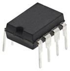
封装:
DIP-8
描述:
Analog Devices### 运算放大器,Analog Devices
Pictures:
3D模型
符号图
焊盘图
引脚图
产品图
页面导航:
原理图在P3
型号编码规则在P5
功能描述在P1
导航目录
AD746JNZ数据手册
Page:
of 8 Go
若手册格式错乱,请下载阅览PDF原文件
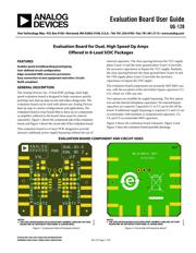
Evaluation Board User Guide
UG-128
One Technology Way • P. O. Box 9106 • Norwood, MA 02062-9106, U.S.A. • Te l: 781.329.4700 • Fax: 781.461.3113 • www.analog.com
Evaluation Board for Dual, High Speed Op Amps
Offered in 8-Lead SOIC Packages
PLEASE SEE THE LAST PAGE FOR AN IMPORTANT
WARNING AND LEGAL TERMS AND CONDITIONS.
Rev. B | Page 1 of 8
FEATURES
Enables quick breadboarding/prototyping
User-defined circuit configuration
Edge-mounted SMA connector provisions
Easy connection to test equipment and other circuits
RoHS compliant
GENERAL DESCRIPTION
The Analog Devices, Inc., 8-lead SOIC package, dual, high
speed evaluation board is designed to help customers quickly
prototype new dual op amp circuits and reduce design time. The
evaluation board can be used with almost any Analog Devices
dual op amp in various configurations and applications. The
evaluation board is a bare board (that is, there are no components
or amplifier soldered to the board; these must be ordered
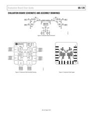
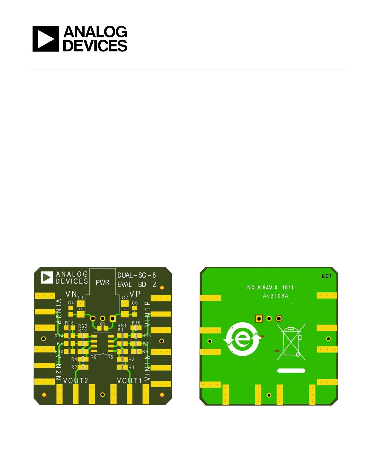
separately). Figure 1 shows the component side of the evaluation
board, and Figure 2 shows the circuit side of the evaluation board.
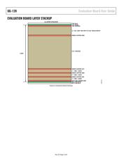
This evaluation board is a 6-layer PCB, designed to provide
internal, wideband, power supply bypassing without the use of
external capacitors. The close spacing between the VCC supply
plane (Layer 3) and the inner ground plane (Layer 4) provides
the necessary capacitance to bypass the VCC supply. Similarly,
the close spacing between the inner ground layer (Layer 4) and
the VEE supply plane (Layer 5) provides the necessary
capacitance to bypass the VEE supply.
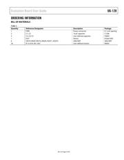
The evaluation board components are primarily SMT 0603 case
size, with the exception of the electrolytic bypass capacitors (C1,
C2), which are 1206 case size.
Two options are available for supply bypassing. The first option
is to use the internal interplanar capacitance. No external bypass
capacitors are required. Capacitors C1 to C5 can be left off the
board. If additional supply bypassing is required, C1 and C2 can
accommodate 1206 tantalum or nonpolarized capacitors. C3,
C4, and C5 accommodate 0603 capacitors.
Figure 3 shows the evaluation board schematic. Figure 4 and
Figure 5 show the evaluation board assembly drawings.
EVALUATION BOARD COMPONENT AND CIRCUIT SIDES
08982-001
NOTES
1. THE EVALUATION BOARD SILKSCREEN PART NUMBER LABELING ON YOUR
BOARD MAY BE DIFFERENT FROM WHAT IS SHOWN HERE.
Figure 1. Component Side of Evaluation Board
08982-002
NOTES
1. THE
E
VALUATION BOARD SILKSCREEN PART NUMBER LABELING ON YOUR
BOARD MAY BE DIFFERENT FROM WHAT IS SHOWN HERE.
Figure 2. Circuit Side of Evaluation Board
器件 Datasheet 文档搜索
AiEMA 数据库涵盖高达 72,405,303 个元件的数据手册,每天更新 5,000 多个 PDF 文件
