Datasheet 搜索 > 接口隔离器 > ADI(亚德诺) > ADN4651BRWZ-RL7 数据手册 > ADN4651BRWZ-RL7 产品设计参考手册 4/12 页
 器件3D模型
¥ 57.712
ADN4651BRWZ-RL7 产品设计参考手册 - ADI(亚德诺)
制造商:
ADI(亚德诺)
分类:
接口隔离器
封装:
SOIC-20
描述:
5 kV rms、600 Mbps双通道LVDS隔离器
Pictures:
3D模型
符号图
焊盘图
引脚图
产品图
页面导航:
典型应用电路图在P1
原理图在P10
应用领域在P4P6P10
电气规格在P11

导航目录
ADN4651BRWZ-RL7数据手册
Page:
of 12 Go
若手册格式错乱,请下载阅览PDF原文件
AN-1177 Application Note
Rev. 0 | Page 4 of 12
CLOCK DISTRIBUTION APPLICATIONS
Differential signaling, such as LVDS, is a good choice for
distributing clock signals around a circuit board. In addition to
the benefits of the common-mode noise immunity of LVDS, a
particular advantage for clock distribution applications is that
radiated emissions are reduced due to the coupling between the
two opposing signals.
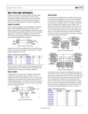
MULTI-DROP CLOCK DISTRIBUTION
In many applications, multiple nodes in a circuit may depend
on a single clock source. A simple approach to distributing
a single clock source to multiple nodes using LVDS, is to use
a multi-drop bus topology as shown in Figure 6. The LVDS
outputs of a clock source are connected to a pair of signal traces
that have short stubs to the various nodes relying on the clock.
11236-006
D
OUT–
D
OUT+
R
IN–
R
IN+
CLK
CLK
CLKCLK
R
T
LVDS
CLOCK
SOURCE
LVDS
CLOCK INPUTS
Figure 6. Multi-Drop LVDS Clock Distribution
The disadvantages of this approach are that the number of
nodes that can be connected is limited and stubs contribute to
degradation of the signal integrity (that is, adding jitter). Stub
lengths and impedances must be carefully controlled.
POINT-TO-POINT CLOCK DISTRIBUTION
A single clock source can be connected to a single node
requiring an LVDS clock input using a point-to-point link.
This can be extended to supply multiple nodes by means of
an LVDS buffer acting as a fan-out device. This separate
component receives the LVDS clock output from the clock
source, and in turn provides this clock signal to multiple LVDS
drivers in the device to drive multiple point-to-point links to
receiving nodes. The advantage of this approach is that timing
on the clock signal can remain unaffected by stubs.
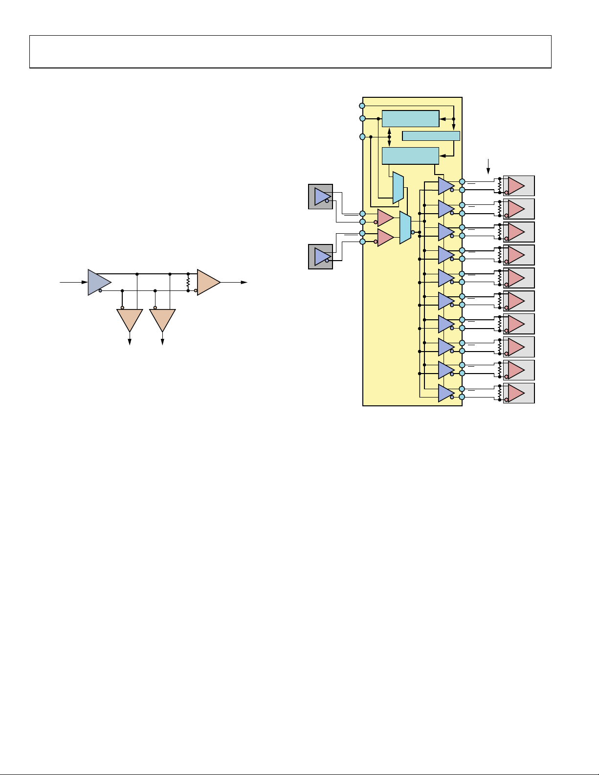
An example of such a device is the ADN4670 clock distribution
buffer. This allows one of two clock sources to be distributed on
up to 10 outputs as shown in Figure 7. The outputs can be
enabled and disabled by means of a serially programmable
register, which is also used to select the clock source.
12-BIT COUNTER
11-BIT SHIFT
REGISTER
11-BIT CONTROL
REGISTER
10 LVDS POINT-
TO-POINT LINKS
Q9
Q8
Q7
Q6
Q5
Q4
Q3
Q2
Q1
Q0
CK
SI
EN
CLK0
CLK1
MUX
MUX
1
0
CLK0
CLK1
Q9
Q8
Q7
Q6
Q5
Q4
Q3
Q2
Q1
Q0
0
1
ADN4670
NODE 9
CLOCK
SOURCE
CLOCK
SOURCE
NODE 0
11236-007
Figure 7. ADN4670 Application Distributing a Clock Source to 10 Nodes via
Point-To-Point LVDS Connections
Any buffer adds a small amount of jitter when inserted between
the initial LVDS output and the eventual LVDS input, but the
ADN4670 has been designed to have low additive jitter of
<300 fs. Skew between the 10 outputs is kept to less than 30 ps
with clock signals of up to 1.1 GHz.
CLOCK DISTRIBUTION USING M-LVDS
Another option for clock distribution is using M-LVDS
transceivers to distribute the clock to up to 32 nodes in a multi-
drop (or multipoint) topology. Type 1 M-LVDS receivers (such
as in the ADN4690E to ADN4693E) are suited to such
applications because there is no offset in the receiver threshold
(this offset can result in duty cycle distortion for a clock signal).
The ADN4690E to ADN4693E M-LVDS transceivers with Type
1 receivers also have additional slew-rate limiting of the edges
from the driver outputs, which further limits radiated emissions
and the effect of reflections from stubs.
器件 Datasheet 文档搜索
AiEMA 数据库涵盖高达 72,405,303 个元件的数据手册,每天更新 5,000 多个 PDF 文件
