Datasheet 搜索 > 微控制器 > ADI(亚德诺) > ADUC7060BSTZ32 数据手册 > ADUC7060BSTZ32 产品设计参考手册 1/12 页

 器件3D模型
¥ 67.667
ADUC7060BSTZ32 产品设计参考手册 - ADI(亚德诺)
制造商:
ADI(亚德诺)
分类:
微控制器
封装:
LQFP-48
描述:
ANALOG DEVICES ADUC7060BSTZ32 微控制器, 32位, 精准模拟, ARM7TDMI, 10 MHz, 32 KB, 4 KB, 48 引脚, LQFP
Pictures:
3D模型
符号图
焊盘图
引脚图
产品图
页面导航:
引脚图在P6Hot
原理图在P8P9
导航目录
ADUC7060BSTZ32数据手册
Page:
of 12 Go
若手册格式错乱,请下载阅览PDF原文件

Evaluation Board User Guide
UG-029
One Technology Way • P. O. Box 9106 • Norwood, MA 02062-9106, U.S.A. • Te l: 781.329.4700 • Fax: 781.461.3113 • www.analog.com
ADuC7060 Evaluation Board User Guide
MicroConverter® ADuC7060 Development System
See the last page for an important warning and disclaimers. Rev. 0 | Page 1 of 12
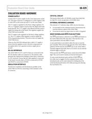
FEATURES
2-layer PCB (4 in. × 5 in. form factor)
9 V power supply regulated to 3.3 V and 2.5 V on board
4-pin UART header to connect to RS-232 interface cable
20-pin standard JTAG connector
Demonstration circuit
32.768 kHz watch crystal to drive the PLL clock
ADR280 1.2 V external reference chip
Reset/download/IRQ0 push buttons
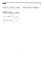
Power indicator/general-purpose LEDs
Access to all ADC inputs and DAC output from external header;
all device ports are brought out to external header pins
Surface-mount and through-hole general-purpose
prototype area
EVALUATION KIT CONTENTS
mIDAS-Link JTAG programming POD
CD containing evaluation software including user manuals,
data sheets, example code, ARMWSD, and evaluation
compilers
9 V power supply
RS-232 to UART cable
USB cable
GENERAL DESCRIPTION
This user guide refers to the ADuC7060 evaluation board.
This evaluation board allows evaluation of the ADuC7060
and ADuC7061 parts. The ADuC7060 is the superset of the
ADuC706x series, and all features of the ADuC7061 can be
evaluated using the ADuC7060. The ADuC7060 contains an
ARM7TDMI core, 32 kB of flash, 4 kB of SRAM, dual 24-bit
sigma-delta (Σ-Δ) ADCs, and a 12-bit DAC as well as many
other features.
This evaluation board allows a user to program the ADuC7060
via the JTAG or the UART interfaces. The user may also debug
their source code through the JTAG interface.
In this user guide, all references to the physical orientation
of components on the board are made with respect to a
component-side view of the board with the prototype area
appearing in the bottom of the board.
The board is laid out to minimize coupling between the analog
and digital sections of the board. To this end, the ground plane
is split with the analog section on the left side and a digital
plane on the right side of the board. The regulated 2.5 V power
supply is routed directly to the digital section and is filtered
before being routed into the analog section of the board.
器件 Datasheet 文档搜索
AiEMA 数据库涵盖高达 72,405,303 个元件的数据手册,每天更新 5,000 多个 PDF 文件
