Datasheet 搜索 > 二极管 > Maxim Integrated(美信) > DS9503P+T&R 数据手册 > DS9503P+T&R 产品设计参考手册 1/11 页

¥ 8.916
DS9503P+T&R 产品设计参考手册 - Maxim Integrated(美信)
制造商:
Maxim Integrated(美信)
分类:
二极管
封装:
LSOJ-6
描述:
MAXIM INTEGRATED PRODUCTS DS9503P+T&R 静电保护装置, TSOC, 6 引脚, 11.05 V
Pictures:
3D模型
符号图
焊盘图
引脚图
产品图
页面导航:
封装尺寸在P1P6
封装信息在P1
导航目录
DS9503P+T&R数据手册
Page:
of 11 Go
若手册格式错乱,请下载阅览PDF原文件

Maxim > Design Support > Technical Documents > Application Notes > General Engineering Topics > APP 3377
Maxim > Design Support > Technical Documents > Application Notes > Prototyping and PC-Board Layout > APP 3377
Keywords: Wafer Level Package, WLP, Flip Chip, Flip-Chip, CSP, Chip Scale Package, PCB Assembly,
PCBA, Die Product, Silicon Circuit, Silicon Die Circuit
APPLICATION NOTE 3377
Maxim Wafer-Level Package Assembly Guide
Nov 12, 2004
Abstract: Wafer-Level Packaging (WLP) allows an integrated circuit (IC) to be attached to a printed-circuit
board (PCB) face-down, with the chip's pads connecting to the PCB pads through individual solder balls. This
document describes the packaging technique and its advantages. It describes printed-circuit board (PCB)
layout and assembly process development for Maxim WLP.
Wafer-Level Packaging (WLP) uses individual solder balls to connect the integrated circuit (IC) to a printed-
circuit board (PCB). The IC is mounted face-down. This technology differs from other ball-grid array, leaded,
and laminate based CSPs because there are no bond wires or interposer connections. The principle
advantage is that IC-to-PCB board inductance is minimized. Secondary benefits are reduction in package size
and manufacturing cycle time, and enhanced thermal conduction characteristics.
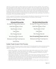
This document describes printed-circuit board (PCB) layout and assembly process development for Maxim
WLP. Note that it is intended for initial PCB layout design and assembly process development and does not
assume any reliability objective for the customer end product. Customers still need to qualify their specified
end product life reliability requirements.
Package Construction
Maxim Package Outlines
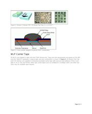
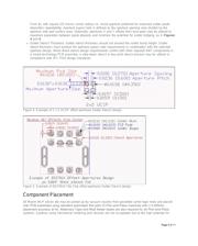
The WLP solder bump interconnect is manufactured by building-up on a silicon wafer substrate. A film of BCB
(Benzocyclobutene) resin is applied over the wafer circuit surface. This film provides mechanical stress relief
for the ball attachment and electrical isolation at the die surface. Vias are imaged in the BCB film, providing
electrical contact to the IC bond pad. A UBM (Under Bump Metal) layer is added over vias. Typically, a
second application of BCB serves as a solder mask to define the diameter and position of reflowed solder
balls. Current package I/O designs include from two up to fifty-five solderable terminals, see Figure 1.
Standard solder bump alloys are eutectic Sn63Pb37, "High-Pb" Pb95Sn5, and "Pb-Free" Sn96.5Ag3Cu0.5. A
cross-section of a single WLP solder bump structure is shown in Figure 2. The backside of the component is
bare silicon with a laser inscribed Pin-1 designator and identification code. A double metal layer redistribution
(RDL) process allows for moving solder bumps from peripheral bond pads to any bump array pattern.
Page 1 of 11
器件 Datasheet 文档搜索
AiEMA 数据库涵盖高达 72,405,303 个元件的数据手册,每天更新 5,000 多个 PDF 文件
