Datasheet 搜索 > Intel(英特尔) > EP2C20F256C7N 数据手册 > EP2C20F256C7N 产品设计参考手册 6/44 页
 器件3D模型
¥ 815.725
EP2C20F256C7N 产品设计参考手册 - Intel(英特尔)
制造商:
Intel(英特尔)
封装:
FBGA-256
Pictures:
3D模型
符号图
焊盘图
引脚图
产品图
页面导航:
原理图在P17
功能描述在P38
应用领域在P5P11

导航目录
EP2C20F256C7N数据手册
Page:
of 44 Go
若手册格式错乱,请下载阅览PDF原文件
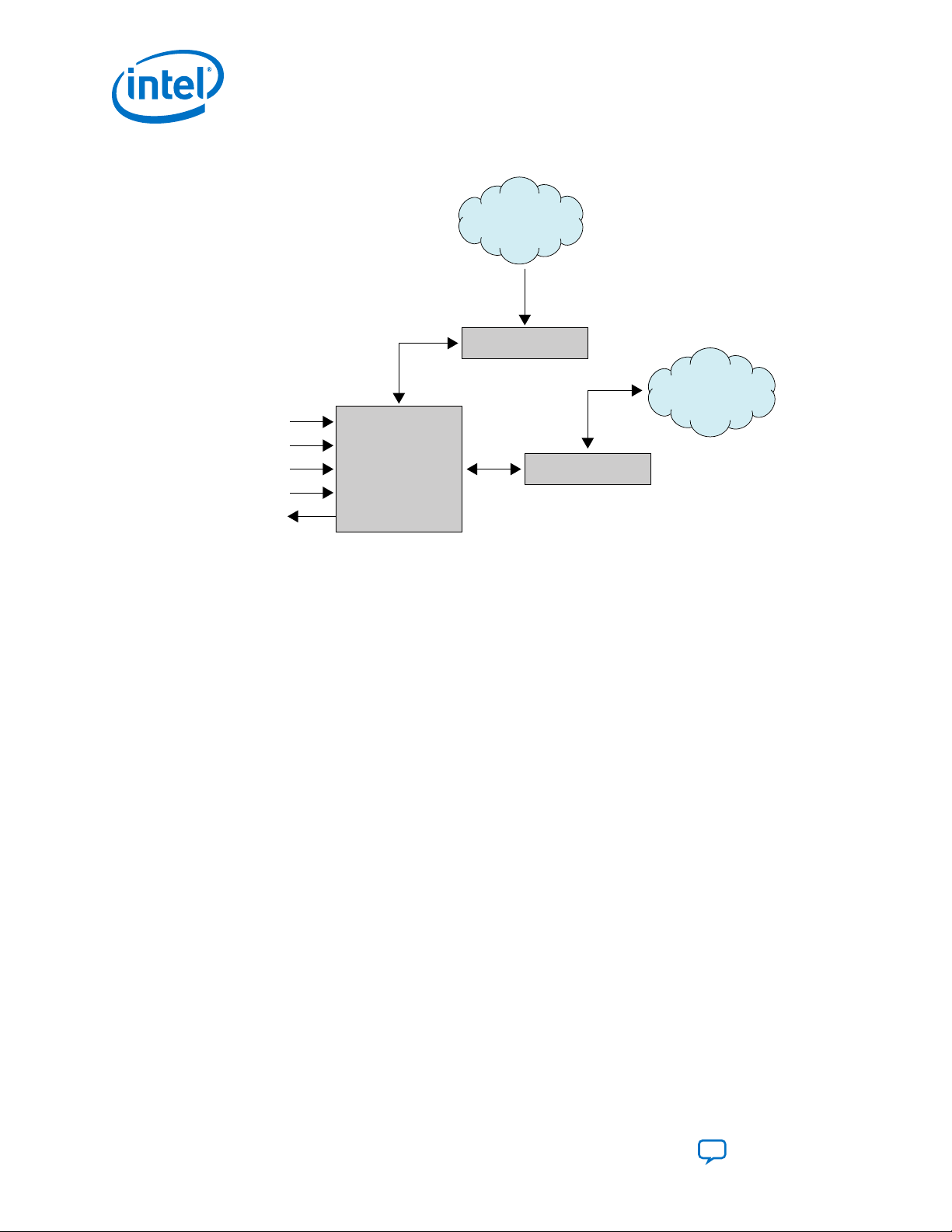
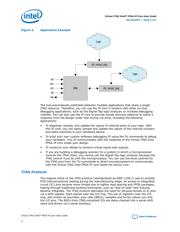
Figure 2. Application Example
Logic
Logic
JTAG
sld_virtual_jtag
sld_virtual_jtag
tck
tms
trst
tdi
tdo
The hub automatically arbitrates between multiple applications that share a single
JTAG resource. Therefore, you can use the IP core in tandem with other on-chip
debugging applications, such as the Signal Tap logic analyzer, to increase debugging
visibility. You can also use the IP core to provide simple stimulus patterns to solicit a
response from the design under test during run-time, including the following
applications:
• To diagnose, sample, and update the values of internal parts of your logic. With
this IP core, you can easily sample and update the values of the internal counters
and state machines in your hardware device.
• To build your own custom software debugging IP using the Tcl commands to debug
your hardware. This IP communicates with the instances of the Virtual JTAG Intel
FPGA IP core inside your design.
• To construct your design to achieve virtual inputs and outputs.
• If you are building a debugging solution for a system in which a microprocessor
controls the JTAG chain, you cannot use the Signal Tap logic analyzer because the
JTAG control must be with the microprocessor. You can use low-level controls for
the JTAG port from the Tcl commands to direct microprocessors to communicate
with the Virtual JTAG Intel FPGA IP core inside the device core.
JTAG Protocol
The original intent of the JTAG protocol (standardized as IEEE 1149.1) was to simplify
PCB interconnectivity testing during the manufacturing stage. As access to integrated
circuit (IC) pins became more limited due to tighter lead spacing and FPGA packages,
testing through traditional probing techniques, such as “bed-of-nails” test fixtures,
became infeasible. The JTAG protocol alleviates the need for physical access to IC pins
via a shift register chain placed near the I/O ring. This set of registers near the I/O
ring, also known as boundary scan cells (BSCs), samples and forces values out onto
the I/O pins. The BSCs from JTAG-compliant ICs are daisy-chained into a serial-shift
chain and driven via a serial interface.
Virtual JTAG Intel
®
FPGA IP Core User Guide
UG-SLDVRTL | 2020.12.01
Virtual JTAG Intel
®
FPGA IP Core User Guide
Send Feedback
6
器件 Datasheet 文档搜索
AiEMA 数据库涵盖高达 72,405,303 个元件的数据手册,每天更新 5,000 多个 PDF 文件
