Datasheet 搜索 > 负载控制器 > ON Semiconductor(安森美) > FDC6331L 数据手册 > FDC6331L 产品设计参考手册 2/8 页

 器件3D模型
¥ 0.855
FDC6331L 产品设计参考手册 - ON Semiconductor(安森美)
制造商:
ON Semiconductor(安森美)
分类:
负载控制器
封装:
TSOT-23-6
描述:
ON Semiconductor FDC6331L 2输出 智能电源开关, 集成负载开关, 2.8A, 8V, 6引脚 SOT-23封装
Pictures:
3D模型
符号图
焊盘图
引脚图
产品图
页面导航:


导航目录
FDC6331L数据手册
Page:
of 8 Go
若手册格式错乱,请下载阅览PDF原文件
Rev. A, August 2001
©2001 Fairchild Semiconductor Corporation
Introduction
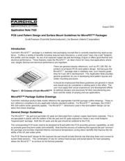
Fairchild’s MicroFET™ package is a relatively new packaging concept that is currently experiencing rapid accep-
tance. It offers a variety of benefits including reduced lead inductance, a small sized "near chip scale" footprint,
thin profile, and low weight. Its use of an exposed copper die-pad technology (Figure 2) offers good thermal and
electrical performance. These features make the MicroFET™ an ideal choice for many new applications where
size, weight, thermal and electrical performance are important.
There are general industry references, such as IPC-SM-782, for
printed circuit board (PCB) land pattern design. But because the
MicroFET™ package style is relatively new, such industry guide-
lines for it are still in development. This Application Note provides
general guidelines for use in developing land pattern layouts and
solder mounting processes.
It should be emphasized that these guidelines are general in nature
and should only be considered a starting point in this effort. The
user must apply their actual experiences and development efforts
to optimize designs and processes for their manufacturing prac-
tices and the needs of varying end-use applications.
MicroFET™ Package Outline Drawings
Fairchild’s individual product data sheets reference the appropriate Fairchild package outline drawings. These in
turn reference compliance to any applicable industry standard outlines. For MicroFET™ packages, the JEDEC
MO-220 outline series generally applies. The MicroFET™ dimensions used in the land pattern design can be
taken from these drawings.
General Design Guidelines
The MicroFET™ die pad and perimeter I/O pads are fabricated from a planar copper lead-frame substrate. This is
encapsulated in plastic with the bottom of the die pad and I/O pads exposed to create a very small footprint
"exposed-pad" package. Both the I/O pads and die pad should be soldered to the PCB.
The corresponding PCB lands need to be designed to fit well within the PCB assembly process capabilities, as well
as promote good long term solder joint reliability. Note that the process of soldering the exposed die pad "anchors"
the package and provides important thermo-mechanical temperature cycling stress benefits that improve the reli-
ability of the I/O pad solder joints.
The PCB "thermal land" design for the exposed die pad should include thermal vias that drop down and connect to
buried metal plane(s). This combination of vias for vertical heat escape and buried planes for heat spreading
allows the MicroFET™ to achieve its full thermal potential.
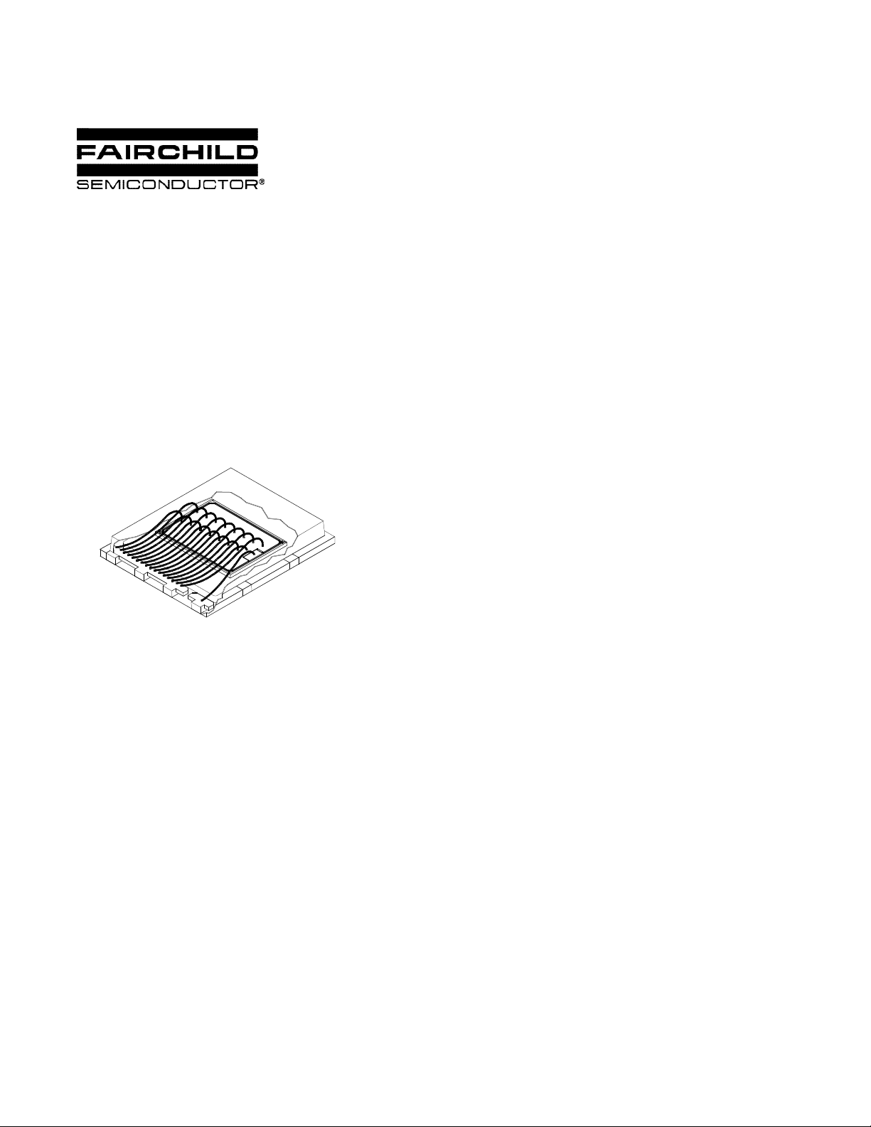
Figure 1. 3D Cutaway of 8 pin MicroFET™
Application Note 7525
PCB Land Pattern Design and Surface Mount Guidelines for MicroFET™ Packages
Scott Pearson (Fairchild Semiconductor), Jim Benson (Intersil Corporation)
August 2001
器件 Datasheet 文档搜索
AiEMA 数据库涵盖高达 72,405,303 个元件的数据手册,每天更新 5,000 多个 PDF 文件
