Datasheet 搜索 > 稳压芯片 > TI(德州仪器) > LM5020SDX-2/NOPB 数据手册 > LM5020SDX-2/NOPB 产品设计参考手册 1/11 页

¥ 8.398
LM5020SDX-2/NOPB 产品设计参考手册 - TI(德州仪器)
制造商:
TI(德州仪器)
分类:
稳压芯片
封装:
WDFN-10
描述:
13V 至 100V 宽输入电压、电流模式 PWM 升压、反激式、Sepic 控制器 10-WSON -40 to 125
Pictures:
3D模型
符号图
焊盘图
引脚图
产品图
页面导航:
应用领域在P11
电气规格在P3P4P5

导航目录
LM5020SDX-2/NOPB数据手册
Page:
of 11 Go
若手册格式错乱,请下载阅览PDF原文件

User's Guide
SNVA082B–March 2004–Revised May 2013
AN-1314 LM5020 Evaluation Board
1 Introduction
The LM5020 evaluation board is designed to provide the design engineer with a fully functional non-
isolated flyback power converter to evaluate the LM5020 controller.
The performance of the evaluation board is as follows:
• Input range: 30V to 75V (100V peak)
• Output voltage: 3.3V
• Output current: 0.2 to 4.5A
• Measured efficiency: 85% at 1.5A, 83% at 4.5A
• Board size: 1.25 × 2.5 × 0.5 inches
• Load Regulation: 1.5%
• Line Regulation: 0.1%
• Line UVLO, Current Limit
The printed circuit board consists of 2 layers of 2 ounce copper on FR4 material with a total thickness of
0.050 inches. Soldermask has been omitted from some areas to facilitate cooling. The unit is designed for
continuous operation at rated load at < 40°C with normal convection cooling.
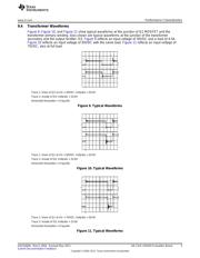
2 Theory of Operation
The flyback converter is an inductive based converter in which inductive energy is stored by applying a
voltage across an inductor in a similar manner to that of a boost converter. Here the similarity ends. A
second coupled winding of the inductor transfers the energy to a secondary side rectifier after the voltage
has been removed from the first winding. This allows the converter input and output grounds to be
configured either isolated or non-isolated. There is also a voltage/current ratio change possible by altering
the winding ratio between the first winding and the second winding. A semi-regulated auxiliary winding can
also be provided.
The flyback transformer is actually a coupled inductor with multiple windings wound on a single core. For
simplification, we will refer to the first, driven winding, as the primary and the main output winding as the
secondary winding of the flyback transformer.
The transformer’s primary inductance is typically made as large as is practical. However, the airgap
necessary to store the cycle energy lowers the obtainable inductance. The higher the primary inductance,
the less input ripple current will be generated and the less input filtering will be required.
As shown, the LM5020 directly drives a MOSFET switch to apply voltage across the primary. When the
switch turns off, the secondary applies a forward current to the output rectifier and charges the output
capacitor. In applications where the input voltage is considerably higher than the output voltage, the turns
ratio between primary and secondary will reflect the input/output voltage ratio and the duty cycle.
The LM5020 is a full-featured controller providing an internal start-up regulator, soft start, over-current and
under-voltage lockout.
All trademarks are the property of their respective owners.
1
SNVA082B–March 2004–Revised May 2013 AN-1314 LM5020 Evaluation Board
Submit Documentation Feedback
Copyright © 2004–2013, Texas Instruments Incorporated
器件 Datasheet 文档搜索
AiEMA 数据库涵盖高达 72,405,303 个元件的数据手册,每天更新 5,000 多个 PDF 文件
