Datasheet 搜索 > 放大器、缓冲器 > Maxim Integrated(美信) > MAX4173FESA+T 数据手册 > MAX4173FESA+T 产品设计参考手册 5/14 页
 器件3D模型
¥ 4.244
MAX4173FESA+T 产品设计参考手册 - Maxim Integrated(美信)
制造商:
Maxim Integrated(美信)
分类:
放大器、缓冲器
封装:
SO-8
描述:
MAX4173FESA+T 编带
Pictures:
3D模型
符号图
焊盘图
引脚图
产品图
页面导航:
原理图在P1
应用领域在P1
导航目录
MAX4173FESA+T数据手册
Page:
of 14 Go
若手册格式错乱,请下载阅览PDF原文件

Feedback
EMI/RFI
High-frequency operation (to 1MHz and higher) of the transformers in today's switching power supplies
allows a reduction in all dimensions of those magnetic components. On the other hand, the high-
frequency square waves (PWM or PFM topologies) or sine waves (resonant or quasi-resonant
topologies) produce electromagnetic emissions during every cycle of energy transfer. International
standards define limits for these emissions, which are conducted by the input and the output cables as
EMI and radiated from space around the power supply as RFI.
The international specification for conducted EMI and radiated RFI is EN55022, which lists maximum
allowable amplitudes for EMI in the range 150kHz to 30MHz (Table 1) and for RFI in the range 30MHz
to 1000MHz (Table 2). EN55022 also defines the tests needed for verifying compliance with its
requirements, and it delineates the conditions necessary for approval of the laboratory in which the tests
are conducted. Products that fail to meet these specifications for electromagnetic compatibility cannot be
branded with the CE mark for sale in the European community or with UL approval for sale in the United
States.
To meet specified limits for EMI and RFI, you must consider certain points during the design. First,
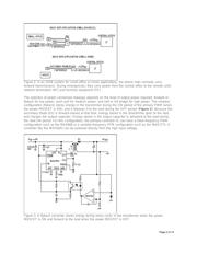
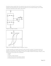
identify sources of noise and minimize them as much as possible. In the 100kHz flyback topology in
Figure 3, for example, five noise sources are easily identified:
1. Rise and fall time at the power MOSFET T1: According to Fourier analysis, this square wave can be
regarded as a sum of harmonics: the first at 100kHz, the second at 200kHz, the third at 300kHz, etc., all
with progressively lower amplitudes. Reducing the switching waveform's dV/dT minimizes the high-
frequency harmonics, but a limit is imposed by the power dissipated during turn-on and turn-off.
2. T1 turn-off: During T1's turn-off, parasitic inductance and capacitance in the circuit and the
transformer cause higher-frequency ringing in the drain voltage. This ringing energy can be minimized by
specifying a transformer with small leakage inductance and by adding a diode/resistor/capacitor snubber
circuit.
3. Ringing in D1: Similarly, an undesired noise frequency (ringing) due to parasitic capacitance in the
secondary diode D1 can be reduced by a resistor/capacitor network in parallel with the diode.
4. RFI from the transformer: RFI noise caused by the flyback transformer's air gap can be reduced
several decibels by shielding the transformer with copper foil.
5. Layout: All components carrying the switching waveform should be as small as possible, with short
connections. A long connection can act as an antenna, transmitting unwanted noise almost everywhere.
In 99% of all cases, you can reduce the problem (but not solve it completely) by taking all these
principles into account. They entail the cost of extra parts. Noise coming from the power supply and
present at the battery input, for example, must be attenuated with an EMI filter that consists of a
differential inductor, a common-mode inductor, and ceramic or high-frequency capacitors. It is
impossible, however, to define a standard series of EMI filters that accommodates all different circuit
topologies and output-power levels.
A number of the elements involved in noise generation are not predictable by analysis. Only when the
power supply has been implemented physically can you perform the analysis and experimental tests that
enable design of the EMI filter. To allow a reasonable spread of component values during production,
Page 5 of 14
器件 Datasheet 文档搜索
AiEMA 数据库涵盖高达 72,405,303 个元件的数据手册,每天更新 5,000 多个 PDF 文件
