Datasheet 搜索 > Microchip(微芯) > MCP3421A4T-E/CH 数据手册 > MCP3421A4T-E/CH 产品设计参考手册 3/30 页


¥ 12.373
MCP3421A4T-E/CH 产品设计参考手册 - Microchip(微芯)
制造商:
Microchip(微芯)
封装:
SOT-23-6
描述:
18位模拟数字转换器,带有I2C接口,并板载参考 18-Bit Analog-to-Digital Converter with I2C Interface and On-Board Reference
Pictures:
3D模型
符号图
焊盘图
引脚图
产品图
页面导航:
引脚图在P6Hot
典型应用电路图在P1P21P22
原理图在P1
标记信息在P23
封装信息在P23P24P27
技术参数、封装参数在P3P18P19
应用领域在P1
电气规格在P3P6P7P18P19P21
导航目录
MCP3421A4T-E/CH数据手册
Page:
of 30 Go
若手册格式错乱,请下载阅览PDF原文件
© 2006 Microchip Technology Inc. DS22003B-page 3
MCP3421
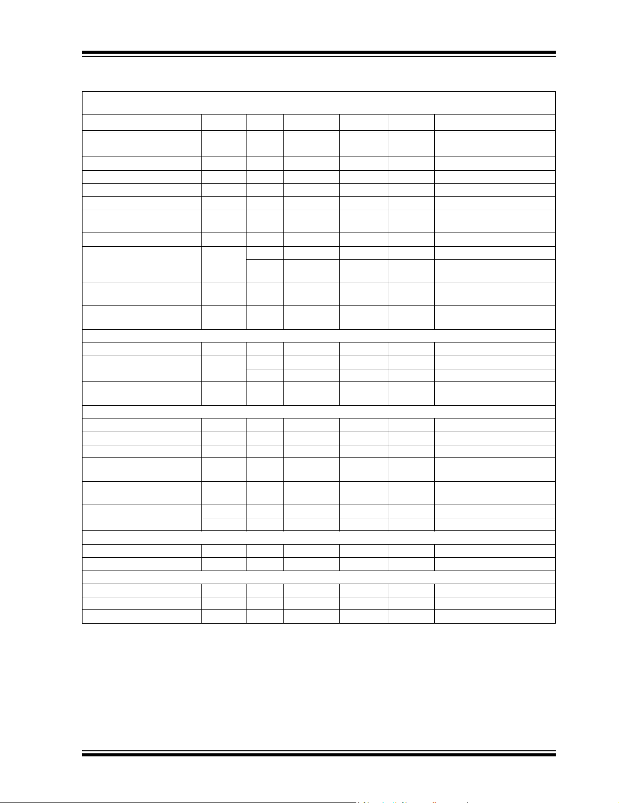
Integral Nonlinearity
(Note 4)
INL — 10 35
ppm of
FSR
DR = 3.75 SPS
(Note 6)
Internal Reference Voltage V
REF
— 2.048 — V
Gain Error
(Note 5)
— 0.05 0.35 % PGA = 1, DR = 3.75 SPS
PGA Gain Error Match
(Note 5)
— 0.1 — % Between any 2 PGA gains
Gain Error Drift
(Note 5)
— 5 40 ppm/°C PGA=1, DR=3.75 SPS
Offset Error V
OS
— 15 40 µV Tested at PGA = 1
V
DD
= 5.0V and DR = 3.75 SPS
Offset Drift vs. Temperature — 50 — nV/°C V
DD = 5.0V
Common-Mode Rejection — 105 — dB at DC and PGA =1,
— 110 — dB at DC and PGA =8,
T
A
= +25°C
Gain vs. V
DD
— 5 — ppm/V T
A
= +25°C, V
DD
= 2.7V to 5.5V,
PGA = 1
Power Supply Rejection at DC — 100 — dB T
A
= +25°C, V
DD
= 2.7V to 5.5V,
PGA = 1
Power Requirements
Voltage Range V
DD
2.7 — 5.5 V
Supply Current during
Conversion
I
DDA
— 155 190 µA V
DD
= 5.0V
— 145 — µA V
DD
= 3.0V
Supply Current during Standby
Mode
I
DDS
—0.1 0.5µA
I
2
C Digital Inputs and Digital Outputs
High level input voltage V
IH
0.7 V
DD
—V
DD
V
Low level input voltage V
IL
— — 0.3V
DD
V
Low level output voltage V
OL
—— 0.4VI
OL
= 3 mA, V
DD
= +5.0V
Hysteresis of Schmitt Trigger
for inputs
(Note 7)
V
HYST
0.05V
DD
——Vf
SCL
= 100 kHz
Supply Current when I
2
C bus
line is active
I
DDB
—— 10µA
Input Leakage Current I
ILH
—— 1 µAV
IH
= 5.5V
I
ILL
-1 — — µA V
IL
= GND
Pin Capacitance and I
2
C Bus Capacitance
Pin capacitance C
PIN
— — 10 pF
I
2
C Bus Capacitance C
b
— — 400 pF
Thermal Characteristics
Specified Temperature Range T
A
-40 — +85 °C
Operating Temperature Range T
A
-40 — +125 °C
Storage Temperature Range T
A
-65 — +150 °C
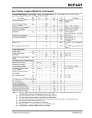
ELECTRICAL CHARACTERISTICS (CONTINUED)
Electrical Specifications: Unless otherwise specified, all parameters apply for T
A
= -40°C to +85°C, V
DD
= +5.0V, V
SS
= 0V,
V
IN
+ = V
IN
- = V
REF
/2. All ppm units use 2*V
REF
as full-scale range.
Parameters Sym Min Typ Max Units Conditions
Note 1: Any input voltage below or greater than this voltage causes leakage current through the ESD diodes at the input pins.
This parameter is ensured by characterization and not 100% tested.
2: This input impedance is due to 3.2 pF internal input sampling capacitor.
3: The total conversion speed includes auto-calibration of offset and gain.
4: INL is the difference between the endpoints line and the measured code at the center of the quantization band.
5: Includes all errors from on-board PGA and V
REF
.
6: Full Scale Range (FSR) = 2 x 2.048/PGA = 4.096/PGA.
7: This parameter is ensured by characterization and not 100% tested.
8: This parameter is ensured by design and not 100% tested.
器件 Datasheet 文档搜索
AiEMA 数据库涵盖高达 72,405,303 个元件的数据手册,每天更新 5,000 多个 PDF 文件
