Datasheet 搜索 > 微处理器 > TI(德州仪器) > OMAP3503DCUS 数据手册 > OMAP3503DCUS 产品设计参考手册 1/264 页
 器件3D模型
¥ 2.48
OMAP3503DCUS 产品设计参考手册 - TI(德州仪器)
制造商:
TI(德州仪器)
分类:
微处理器
封装:
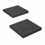
FCBGA-423
Pictures:
3D模型
符号图
焊盘图
引脚图
产品图
页面导航:
引脚图在P5P13Hot
原理图在P4P176P177P178
封装尺寸在P258P259
标记信息在P258P259P260
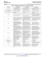
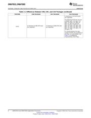
封装信息在P3P255P256P257P258P259P260
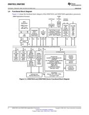
功能描述在P195
技术参数、封装参数在P3P120P133P134P135P136P137P138P139P140P141P142
应用领域在P1P2P3P4P5P6P9P10P11P12P13P134
电气规格在P3P118P119P120P121P122P123P124P125P126P127P128
导航目录
OMAP3503DCUS数据手册
Page:
of 264 Go
若手册格式错乱,请下载阅览PDF原文件
OMAP3515, OMAP3503
www.ti.com
SPRS505H –FEBRUARY 2008–REVISED OCTOBER 2013
OMAP3515 and OMAP3503 Applications Processors
Check for Samples: OMAP3515, OMAP3503
1 OMAP3515 and OMAP3503 Applications Processors
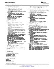
1.1 Features
12
– 256-KB L2 Cache
• OMAP3515 and OMAP3503 Devices:
• 112KB of ROM
– OMAP™ 3 Architecture
• 64KB of Shared SRAM
– MPU Subsystem
• Endianess:
• Up to 720-MHz ARM® Cortex™-A8 Core
– ARM Instructions – Little Endian
• NEON™ SIMD Coprocessor
– ARM Data – Configurable
– PowerVR® SGX™ Graphics Accelerator
(OMAP3515 Device Only) • External Memory Interfaces:
• Tile-Based Architecture Delivering up to – SDRAM Controller (SDRC)
10 MPoly/sec
• 16- and 32-Bit Memory Controller with
• Universal Scalable Shader Engine: Multi- 1GB of Total Address Space
threaded Engine Incorporating Pixel and
• Interfaces to Low-Power Double Data
Vertex Shader Functionality
Rate (LPDDR) SDRAM
• Industry Standard API Support:
• SDRAM Memory Scheduler (SMS) and
OpenGLES 1.1 and 2.0, OpenVG1.0
Rotation Engine
• Fine-Grained Task Switching, Load
– General Purpose Memory Controller (GPMC)
Balancing, and Power Management
• 16-Bit-Wide Multiplexed Address and
• Programmable High-Quality Image Anti-
Data Bus
Aliasing
• Up to 8 Chip-Select Pins with 128-MB
– Fully Software-Compatible with ARM9™
Address Space per Chip-Select Pin
– Commercial and Extended Temperature
• Glueless Interface to NOR Flash, NAND
Grades
Flash (with ECC Hamming Code
• ARM Cortex-A8 Core Calculation), SRAM, and Pseudo-SRAM
– ARMv7 Architecture • Flexible Asynchronous Protocol Control
for Interface to Custom Logic (FPGA,
• TrustZone®
CPLD, ASICs, and so forth)
• Thumb®-2
• Nonmultiplexed Address and Data Mode
• MMU Enhancements
(Limited 2-KB Address Space)
– In-Order, Dual-Issue, Superscalar
• System Direct Memory Access (sDMA)
Microprocessor Core
Controller (32 Logical Channels with
– NEON Multimedia Architecture
Configurable Priority)
– Over 2x Performance of ARMv6 SIMD
• Camera Image Signal Processor (ISP)
– Supports Both Integer and Floating-Point
– CCD and CMOS Imager Interface
SIMD
– Memory Data Input
– Jazelle® RCT Execution Environment
– BT.601 (8-Bit) and BT.656 (10-Bit) Digital
Architecture
YCbCr 4:2:2 Interface
– Dynamic Branch Prediction with Branch
– Glueless Interface to Common Video
Target Address Cache, Global History
Decoders
Buffer, and 8-Entry Return Stack
– Resize Engine
– Embedded Trace Macrocell (ETM) Support
• Resize Images From 1/4x to 4x
for Noninvasive Debug
• Separate Horizontal and Vertical Control
• ARM Cortex-A8 Memory Architecture:
• Display Subsystem
– 16-KB Instruction Cache (4-Way Set-
Associative) – Parallel Digital Output
– 16-KB Data Cache (4-Way Set-Associative) • Up to 24-Bit RGB
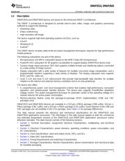
1
Please be aware that an important notice concerning availability, standard warranty, and use in critical applications of
Texas Instruments semiconductor products and disclaimers thereto appears at the end of this data sheet.
2All trademarks are the property of their respective owners.
PRODUCTION DATA information is current as of publication date. Products conform to
Copyright © 2008–2013, Texas Instruments Incorporated
specifications per the terms of the Texas Instruments standard warranty. Production
processing does not necessarily include testing of all parameters.
器件 Datasheet 文档搜索
AiEMA 数据库涵盖高达 72,405,303 个元件的数据手册,每天更新 5,000 多个 PDF 文件
