Datasheet 搜索 > LED驱动器 > TI(德州仪器) > TLC5940PWPG4 数据手册 > TLC5940PWPG4 产品设计参考手册 4/18 页
 器件3D模型
¥ 6.74
TLC5940PWPG4 产品设计参考手册 - TI(德州仪器)
制造商:
TI(德州仪器)
分类:
LED驱动器
封装:
HTSSOP-28
描述:
16通道LED驱动器,具有点校正和灰度PWM控制 16 CHANNEL LED DRIVER WITH DOT CORRECTION AND GRAYSCALE PWM CONTROL
Pictures:
3D模型
符号图
焊盘图
引脚图
产品图
页面导航:
原理图在P13P14P15P16
应用领域在P18

导航目录
TLC5940PWPG4数据手册
Page:
of 18 Go
若手册格式错乱,请下载阅览PDF原文件
www.ti.com
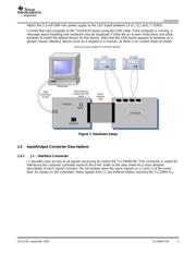
Introduction
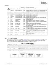
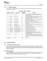
Table 1. J1 – Interface Connector
Pin
Pin Symbol Signal Name I/O Function
Number
1 SIN_RED Serial data input red Input Serial data input for the red LED IC. This is also the serial data input
when all three TLC5940 ICs are connected in cascade mode
(serially).
2 SOUT_R Serial data output red Output Serial data output from the red LED IC
3 SIN_GREEN Serial data input green Input Serial data input for the green LED IC
4 SOUT_G Serial data output green Output Serial data output for the green LED IC
5 SIN_BLUE Serial data input blue Input Serial data input for the blue LED IC
6 SOUT_B Serial data output blue Output Serial data output for the blue LED IC. This is also the serial data
output in cascade mode.
7 SCLK Serial data clock Input Serial data input clock
8 XLAT Data latch Input Rising edge latches data from shift register into the device
9 BLANK Output enable Input Output enable for all channels. Outputs are disabled when BLANK is
high.
10 GSCLK GS PWM Clock Input Grayscale clock signal for 12-bit PWM dimming
11 DCPRG DC PRG Mode Input Selects either the internal register or the internal EEPROM when in
DOT correction mode.
12 XDOWN Error signal Output Error flag (LOD and TEF) output. Note: XDOWN signal of all three
devices is tied together.
13 VPRG_IN VPRG Signal Input This signal is buffered and combined with the /22V_EN signal to set
the VPRG voltage on the TLC5940 ICs.
14 /22V_EN 22V Enable Input This is an active low enable signal that turns on the 22V power
supply that is used to program the internal EEPROM on the
TLC5940 ICs.
15 BUF_EN Buffer enable signal Input This is an active low enable signal that turns on the buffer for the
control signals on the EVM.
16 GND Ground Power Signal ground
1.3.2 J2 – Power Connector
This connector supplies power to the EVM. Table 2 shows pin assignments and Table 3 shows the power
requirements of the EVM. Ensure that the input power has the required current capability. The power
inputs to this connector are identical to the power inputs on J4, J5, J6, and J7.
Table 2. J2 – Power Connector
Pin Number Pin Symbol Function
1, 2 V_CC Supplies bias power for the ICs on the EVM board
3, 4, 5, 6, 11, 12 GND Power ground
7, 8 V_GB Supplies power to drive the LEDs. V_GB is connected to the anode of all three colors of each
RGB LED.
9, 10 V_R Not connected
Table 3. EVM Power Requirements
Pin Number Pin Symbol Voltage Range Max Current
1, 2 V_CC 3.3 V ± 0.1 V > 500 mA
7, 8 V_GB 4.0 V – 17 V > 2000 mA
TLC5940 EVM4 SLVU139 – September 2005
器件 Datasheet 文档搜索
AiEMA 数据库涵盖高达 72,405,303 个元件的数据手册,每天更新 5,000 多个 PDF 文件
