Datasheet 搜索 > 开发板 > TI(德州仪器) > TMDX5505EZDSP 数据手册 > TMDX5505EZDSP 产品设计参考手册 2/157 页

¥ 2577.691
TMDX5505EZDSP 产品设计参考手册 - TI(德州仪器)
制造商:
TI(德州仪器)
分类:
开发板
描述:
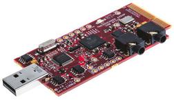
TMS320VC550x DSP 开发工具TMDX5505eZDSP 是小型设计、成本极低、USB 供电 DSP 开发工具,包括评估 TMS320VC5504 和 TMS320VC5505 DSP 所需的所有硬件和软件。 USB 端口提供足够的功率运行超低功耗 C5505,因此无需外部电源。 此工具可以快速轻松评估 C5505 和 C5504 处理器的先进功能。 它具有嵌入式 XDS510 仿真器,用于完全源码级调试功能且支持 Code Composer Studio™ 旋转。 4.0 IDE 和 eXpressDSP™ 软件,包括 DSP/BIOSv 内核。TMS320VC5505 定点低功率 DSP 嵌入式 XDS100 仿真器 I²C 串行 EEPROM TLV320AIC3204 32 位可编程低功率立体声编码解码器 输入、耳机输出连接器 扩展连接器 可拆卸 USB 棒外壳 ### 随附Code Composer Studio™ 4.0、DSP/BIOS™ 实时内核、芯片支持库### 数字信号处理器,Texas Instruments
Pictures:
3D模型
符号图
焊盘图
引脚图
产品图
页面导航:
引脚图在P15P56P59Hot
典型应用电路图在P133
原理图在P4
封装尺寸在P154
标记信息在P154
封装信息在P153P154P155
功能描述在P56
技术参数、封装参数在P12P65P70P71P72P73P74P75P76P77P78P79
应用领域在P2
电气规格在P12P38P43P63P67P68P69P70P71P72P73P74


导航目录
TMDX5505EZDSP数据手册
Page:
of 157 Go
若手册格式错乱,请下载阅览PDF原文件

TMS320C5505
SPRS660F –AUGUST 2010–REVISED SEPTEMBER 2013
www.ti.com
1.2 Applications
• Wireless Audio Devices (Headsets, Microphones, Speakerphones)
• Echo Cancellation Headphones
• Portable Medical Devices
• Voice Applications
• Industrial Controls
• Fingerprint Biometrics
• Software Defined Radio
1.3 Description
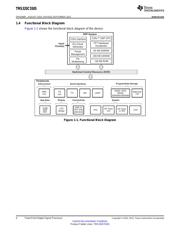
The device is a member of TI's TMS320C5000™ fixed-point Digital Signal Processor (DSP) product family
and is designed for low-power applications.
The fixed-point DSP is based on the TMS320C55x™ DSP generation CPU processor core. The C55x™
DSP architecture achieves high performance and low power through increased parallelism and total focus
on power savings. The CPU supports an internal bus structure that is composed of one program bus, one
32-bit data read bus and two 16-bit data read buses, two 16-bit data write buses, and additional buses
dedicated to peripheral and DMA activity. These buses provide the ability to perform up to four 16-bit data
reads and two 16-bit data writes in a single cycle. The device also includes four DMA controllers, each
with 4 channels, providing data movement for 16-independent channel contexts without CPU intervention.
Each DMA controller can perform one 32-bit data transfer per cycle, in parallel and independent of the
CPU activity.
The C55x CPU provides two multiply-accumulate (MAC) units, each capable of 17-bit x 17-bit
multiplication and a 32-bit add in a single cycle. A central 40-bit arithmetic/logic unit (ALU) is supported by
an additional 16-bit ALU. Use of the ALUs is under instruction set control, providing the ability to optimize
parallel activity and power consumption. These resources are managed in the Address Unit (AU) and Data
Unit (DU) of the C55x CPU.
The C55x CPU supports a variable byte width instruction set for improved code density. The Instruction
Unit (IU) performs 32-bit program fetches from internal or external memory and queues instructions for the
Program Unit (PU). The Program Unit decodes the instructions, directs tasks to the Address Unit (AU) and
Data Unit (DU) resources, and manages the fully protected pipeline. Predictive branching capability avoids
pipeline flushes on execution of conditional instructions.
The general-purpose input and output functions along with the 10-bit SAR ADC provide sufficient pins for
status, interrupts, and bit I/O for LCD displays, keyboards, and media interfaces. Serial media is supported
through two MultiMedia Card/Secure Digital (MMC/SD) peripherals, four Inter-IC Sound (I2S Bus™)
modules, one Serial-Port Interface (SPI) with up to 4 chip selects, one I2C multi-master and slave
interface, and a Universal Asynchronous Receiver/Transmitter (UART) interface.
The device peripheral set includes an external memory interface (EMIF) that provides glueless access to
asynchronous memories like EPROM, NOR, NAND, and SRAM, as well as to high-speed, high-density
memories such as synchronous DRAM (SDRAM) and mobile SDRAM (mSDRAM). Additional peripherals
include: a high-speed Universal Serial Bus (USB2.0) device mode only, and a real-time clock (RTC). This
device also includes three general-purpose timers with one configurable as a watchdog timer, and an
analog phase-locked loop (APLL) clock generator.
In addition, the device includes a tightly-coupled FFT Hardware Accelerator. The tightly-coupled FFT
Hardware Accelerator supports 8 to 1024-point (in power of 2) real and complex-valued FFTs.
The device includes one integrated LDO (ANA_LDO) to provide regulated 1.3 V to the DSP PLL
(V
DDA_PLL
) and 10-bit SAR ADC(V
DDA_ANA
). Note: ANA_LDO can only provide a regulated 1.3 V. When the
DSP PLL requires 1.4 V (PLLOUT > 120 MHz), an external supply is required to supply 1.4 V to the DSP
PLL (V
DDA_PLL
).
2 Fixed-Point Digital Signal Processor Copyright © 2010–2013, Texas Instruments Incorporated
Submit Documentation Feedback
Product Folder Links: TMS320C5505
器件 Datasheet 文档搜索
AiEMA 数据库涵盖高达 72,405,303 个元件的数据手册,每天更新 5,000 多个 PDF 文件
