Datasheet 搜索 > DSP数字信号处理器 > TI(德州仪器) > TMS320C6711DGDP250 数据手册 > TMS320C6711DGDP250 产品设计参考手册 3/109 页
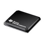
 器件3D模型
¥ 219.993
TMS320C6711DGDP250 产品设计参考手册 - TI(德州仪器)
制造商:
TI(德州仪器)
分类:
DSP数字信号处理器
封装:
BGA-272
描述:
数字信号处理器 (DSP),Texas Instruments德州仪器数字信号处理器是微处理器,带有一个优化的体系结构,用于数字信号处理的运算需求。### 数字信号处理器,Texas Instruments
Pictures:
3D模型
符号图
焊盘图
引脚图
产品图
页面导航:
导航目录
TMS320C6711DGDP250数据手册
Page:
of 109 Go
若手册格式错乱,请下载阅览PDF原文件

SPRS292B − OCTOBER 2005 − REVISED JUNE 2006
3
POST OFFICE BOX 1443 • HOUSTON, TEXAS 77251−1443
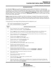
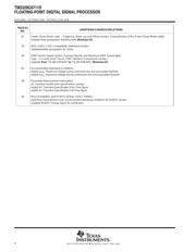
REVISION HISTORY
The TMS320C6711D device-specific documentation has been split from TMS320C6711, TMS320C6711B,
TMS320C6711C, TMS320C6711D Floating−Point Digital Signal Processors, literature number SPRS088N, into a
separate Data Sheet, literature number SPRS292. It also highlights technical changes made to SPRS292 to gen-
erate SPRS292A. These changes are marked by “[Revision A].” Additionally, made changes to SPRS292A to
generate SPRS292B. These changes are marked by “[Revision B].” Both Revision A and B changes are noted
in the Revision History table below.
Scope: Updated information on McBSP and JTAG for clarification. Changed Pin Description for A12 and B11
(Revisions SPRS292 and SPRS292A). Updated Nomenclature figure by adding device−specific information for
the ZDP package. Updated Characteristics of the Processor table with device−specific information (footnote) for
the ZDP package
TI Recommends for new designs that the following pins be configured as such:
D Pin A12 connected directly to CV
DD
(core power)
D Pin B11 connected directly to V
ss
(ground)
PAGE(S)
NO.
ADDITIONS/CHANGES/DELETIONS
21 Device Configurations, device configurations at device reset:
Updated “For proper device operation...” paragraph [Revision B]
22 Device Configurations, Device Configurations Pins at Device Reset (HD[4:3], HD8, HD12, and CLKMODE0) section:
Removed “CE1
width 32−bit” from Functional Description for “00” in HD[4:3](BOOTMODE) Configuration Pin
22 Device Configurations, Device Configurations Pins at Device Reset (HD[4:3], HD8, HD12, and CLKMODE0) section:
Updated “All other HD pins...” footnote [Revision B]
26 Terminal Functions, Resets and Interrupts section:
Updated IPU/IPD for RESET
Signal Name from “IPU” to “−−”
27 Terminal Functions, Host Port Interface, Description section:
Updated “Other HD pins...” paragraph [Revision B]
27 Terminal Functions, Host Port Interface section:
Removed “CE1
width 32−bit” from Description for “00” in Bootmode HD[4:3]
32 Terminal Functions, Reserved for Test section:
Updated Description for RSV Signal Name, A12 GDP/ZDP
Updated Description for RSV Signal Name, B11 GDP/ZDP
32 Terminal Functions, Reserved for Test section:
Updated/changed Description for RSV Signal Name, A12 GDP (to “recommended”) − [Revision A]
Updated/changed Description for RSV Signal Name, B11 GDP (to “recommended”) − [Revision A]
39 Device Support, device and development-support tool nomenclature:
Updated figure for clarity
40 Device Support, documentation support section:
Updated paragraphs for clarity
55 Power−Down Mode Logic − Triggering, Wake−up and Effects section:
Updated paragraphs [Revision B]
57 Power−Down Mode Logic − Triggering, Wake−up and Effects section, Characteristics of the Power-Down Modes table:
Added “It is recommended to use the PLLPWDN bit (PLLCSR.1) as an alternative to PD3” to PRWD Field (BITS 15−10) −
011100 − Effect on Chip’s Operation [Revision B]
器件 Datasheet 文档搜索
AiEMA 数据库涵盖高达 72,405,303 个元件的数据手册,每天更新 5,000 多个 PDF 文件
