Datasheet 搜索 > DSP数字信号处理器 > TI(德州仪器) > TMS320C6745DPTPA3 数据手册 > TMS320C6745DPTPA3 产品设计参考手册 3/1469 页
 器件3D模型
¥ 146.561
TMS320C6745DPTPA3 产品设计参考手册 - TI(德州仪器)
制造商:
TI(德州仪器)
分类:
DSP数字信号处理器
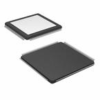
封装:
LQFP-176
描述:
TMS320C6745 , TMS320C6747固定/浮点数字信号处理器 TMS320C6745,TMS320C6747 Fixed/Floating-Point Digital Signal Processor
Pictures:
3D模型
符号图
焊盘图
引脚图
产品图
页面导航:
引脚图在P695P699P780P784P785P880P1039P1041Hot
典型应用电路图在P1169
原理图在P66P67P69P78P83P248P249P291P400P401P438P441
功能描述在P399
应用领域在P174P253P254P255P256P257P258P259P260P261P262P263
导航目录
TMS320C6745DPTPA3数据手册
Page:
of 1469 Go
若手册格式错乱,请下载阅览PDF原文件

www.ti.com
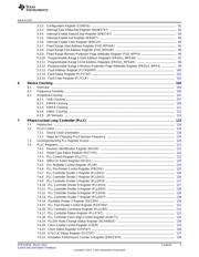
5.3.2 Configuration Register (CONFIG) .............................................................................. 91
5.3.3 Interrupt Raw Status/Set Register (IRAWSTAT) ............................................................. 92
5.3.4 Interrupt Enable Status/Clear Register (IENSTAT) .......................................................... 93
5.3.5 Interrupt Enable Set Register (IENSET) ....................................................................... 94
5.3.6 Interrupt Enable Clear Register (IENCLR) .................................................................... 94
5.3.7 Fixed Range Start Address Register (FXD_MPSAR) ....................................................... 95
5.3.8 Fixed Range End Address Register (FXD_MPEAR) ........................................................ 95
5.3.9 Fixed Range Memory Protection Page Attributes Register (FXD_MPPA) ................................ 96
5.3.10 Programmable Range n Start Address Registers (PROGn_MPSAR) .................................... 97
5.3.11 Programmable Range n End Address Registers (PROGn_MPEAR) .................................... 98
5.3.12 Programmable Range n Memory Protection Page Attributes Register (PROGn_MPPA) ............. 99
5.3.13 Fault Address Register (FLTADDRR) ....................................................................... 100
5.3.14 Fault Status Register (FLTSTAT) ............................................................................ 101
5.3.15 Fault Clear Register (FLTCLR) .............................................................................. 102
6 Device Clocking ............................................................................................................... 103
6.1 Overview .................................................................................................................. 104
6.2 Frequency Flexibility ..................................................................................................... 105
6.3 Peripheral Clocking ...................................................................................................... 107
6.3.1 USB Clocking .................................................................................................... 107
6.3.2 EMIFB Clocking ................................................................................................. 109
6.3.3 EMIFA Clocking ................................................................................................. 111
6.3.4 EMAC Clocking .................................................................................................. 112
6.3.5 I/O Domains ..................................................................................................... 114
7 Phase-Locked Loop Controller (PLLC) ............................................................................... 115
7.1 Introduction ............................................................................................................... 116
7.2 PLL0 Control .............................................................................................................. 116
7.2.1 Device Clock Generation ....................................................................................... 118
7.2.2 Steps for Changing PLL0 Domain Frequency .............................................................. 119
7.3 Locking/Unlocking PLL Register Access .............................................................................. 120
7.4 PLLC Registers ........................................................................................................... 121
7.4.1 Revision Identification Register (REVID) .................................................................... 122
7.4.2 Reset Type Status Register (RSTYPE) ...................................................................... 122
7.4.3 PLL Control Register (PLLCTL) ............................................................................... 123
7.4.4 OBSCLK Select Register (OCSEL) ........................................................................... 124
7.4.5 PLL Multiplier Control Register (PLLM) ...................................................................... 125
7.4.6 PLL Pre-Divider Control Register (PREDIV) ................................................................ 125
7.4.7 PLL Controller Divider 1 Register (PLLDIV1) ............................................................... 126
7.4.8 PLL Controller Divider 2 Register (PLLDIV2) ............................................................... 126
7.4.9 PLL Controller Divider 3 Register (PLLDIV3) ............................................................... 127
7.4.10 PLL Controller Divider 4 Register (PLLDIV4) .............................................................. 127
7.4.11 PLL Controller Divider 5 Register (PLLDIV5) .............................................................. 128
7.4.12 PLL Controller Divider 6 Register (PLLDIV6) .............................................................. 128
7.4.13 PLL Controller Divider 7 Register (PLLDIV7) .............................................................. 129
7.4.14 Oscillator Divider 1 Register (OSCDIV) ..................................................................... 130
7.4.15 PLL Post-Divider Control Register (POSTDIV) ............................................................ 131
7.4.16 PLL Controller Command Register (PLLCMD) ............................................................ 131
7.4.17 PLL Controller Status Register (PLLSTAT) ................................................................ 132
7.4.18 PLL Controller Clock Align Control Register (ALNCTL) .................................................. 133
7.4.19 PLLDIV Ratio Change Status Register (DCHANGE) ..................................................... 134
7.4.20 Clock Enable Control Register (CKEN) ..................................................................... 135
7.4.21 Clock Status Register (CKSTAT) ............................................................................ 136
7.4.22 SYSCLK Status Register (SYSTAT) ........................................................................ 137
7.4.23 Emulation Performance Counter 0 Register (EMUCNT0) ................................................ 138
3
SPRUH91B–March 2013 Contents
Submit Documentation Feedback
Copyright © 2013, Texas Instruments Incorporated
器件 Datasheet 文档搜索
AiEMA 数据库涵盖高达 72,405,303 个元件的数据手册,每天更新 5,000 多个 PDF 文件
