Datasheet 搜索 > DSP数字信号处理器 > TI(德州仪器) > TMS320DM365ZCE30 数据手册 > TMS320DM365ZCE30 产品设计参考手册 1/211 页

¥ 40.025
TMS320DM365ZCE30 产品设计参考手册 - TI(德州仪器)
制造商:
TI(德州仪器)
分类:
DSP数字信号处理器
封装:
LFBGA-338
描述:
TEXAS INSTRUMENTS TMS320DM365ZCE30 芯片, 数字媒体系统, 338NFBGA
Pictures:
3D模型
符号图
焊盘图
引脚图
产品图
页面导航:
引脚图在P16P21P22P23P24P25P26P27P28P29P30P31Hot
典型应用电路图在P47
原理图在P4P9P53P107P109P110
封装尺寸在P207
标记信息在P207
封装信息在P206P207P208
技术参数、封装参数在P71P76P77P78P79P80P81P82P83P84P85P86
应用领域在P210
电气规格在P74P76P77P78P79P80P81P82P83P84P85P86
导航目录
TMS320DM365ZCE30数据手册
Page:
of 211 Go
若手册格式错乱,请下载阅览PDF原文件

TMS320DM365
www.ti.com
SPRS457E–MARCH 2009–REVISED JUNE 2011
TMS320DM365
Digital Media System-on-Chip (DMSoC)
Check for Samples: TMS320DM365
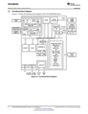
1 TMS320DM365 Digital Media System-on-Chip (DMSoC)
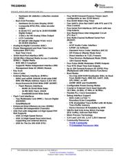
1.1 Features
12
– Support for 32-Bit and 16-Bit
• Highlights
(Thumb® Mode) Instruction Sets
– High-Performance Digital Media
– DSP Instruction Extensions and Single Cycle
System-on-Chip (DMSoC)
MAC
– Up to 300-MHz ARM926EJ-S Clock Rate
– ARM® Jazelle® Technology
– Two Video Image Co-processors
– Embedded ICE-RT Logic for Real-Time
(HDVICP, MJCP) Engines
Debug
– Supports a Range of Encode, Decode, and
• ARM9 Memory Architecture
Video Quality Operations
– 16K-Byte Instruction Cache
– Video Processing Subsystem
– 8K-Byte Data Cache
• HW Face Detect Engine
– 32K-Byte RAM
• Resize Engine from 1/16x to 8x
– 16K-Byte ROM
• 16-Bit Parallel AFE (Analog Front-End)
Interface Up to 120 MHz – Little Endian
• 4:2:2 (8-/16-bit) Interface • Two Video Image Co-processors
(HDVICP, MJCP) Engines
• 8-/16-bit YCC and Up to 24-Bit RGB888
Digital Output – Support a Range of Encode and Decode
Operations, up to D1 on 216-MHz device and
• 3 DACs for HD Analog Video Output
up to 720p on the 270- and 300-MHz parts
• Hardware On-Screen Display (OSD)
– H.264, MPEG4, MPEG2, MJPEG, JPEG,
– Capable of 720p 30fps H.264 video
WMV9/VC1
processing
• Video Processing Subsystem
Note: 216-MHz is only capable of D1
processing – Front End Provides:
– Peripherals include EMAC, USB 2.0 OTG, • HW Face Detect Engine
DDR2/NAND, 5 SPIs, 2 UARTs, 2
• Hardware IPIPE for Real-Time Image
MMC/SD/SDIO, Key Scan
Processing
– 8 Different Boot Modes and Configurable
– Resize Engine
Power-Saving Modes
– Resize Images From 1/16x to 8x
– Pin-to-pin and software compatible with
– Separate Horizontal/Vertical
DM368
Control
– Extended temperature (-40ºC – 85ºC)
– Two Simultaneous Output Paths
available for 300-MHz device
• IPIPE Interface (IPIPEIF)
– 3.3-V and 1.8-V I/O, 1.2-V/1.35-V Core
• Image Sensor Interface (ISIF) and CMOS
– 338-Pin Ball Grid Array at 65nm Process
Imager Interface
Technology
• 16-Bit Parallel AFE (Analog Front End)
• High-Performance Digital Media
Interface Up to 120 MHz
System-on-Chip (DMSoC)
• Glueless Interface to Common Video
– 216-, 270-, 300-MHz ARM926EJ-S Clock Rate
Decoders
– Fully Software-Compatible With ARM9™
• BT.601/BT.656/BT.1120 Digital YCbCr
– Extended temperature available for 300-MHz
4:2:2 (8-/16-Bit) Interface
device
• Histogram Module
• ARM926EJ-S™ Core
• Lens distortion correction module (LDC)
1
Please be aware that an important notice concerning availability, standard warranty, and use in critical applications of Texas
Instruments semiconductor products and disclaimers thereto appears at the end of this data sheet.
2All trademarks are the property of their respective owners.
PRODUCTION DATA information is current as of publication date.
Copyright © 2009–2011, Texas Instruments Incorporated
Products conform to specifications per the terms of the Texas
Instruments standard warranty. Production processing does not
necessarily include testing of all parameters.
器件 Datasheet 文档搜索
AiEMA 数据库涵盖高达 72,405,303 个元件的数据手册,每天更新 5,000 多个 PDF 文件
