Datasheet 搜索 > 微控制器 > TI(德州仪器) > TMS320F2809PZQ 数据手册 > TMS320F2809PZQ 产品设计参考手册 6/147 页
 器件3D模型
¥ 7.191
TMS320F2809PZQ 产品设计参考手册 - TI(德州仪器)
制造商:
TI(德州仪器)
分类:
微控制器
封装:
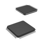
LQFP-100
描述:
TEXAS INSTRUMENTS TMS320F2809PZQ 微控制器, 32位, 36 KB, 100 引脚, LQFP
Pictures:
3D模型
符号图
焊盘图
引脚图
产品图
页面导航:
引脚图在P13P64P65Hot
典型应用电路图在P39P75
原理图在P24P46P58P60P63P68P74P78P81
封装尺寸在P138P139P140P141
标记信息在P138P139P140P141P142
封装信息在P11P12P138P139P140P141P142
技术参数、封装参数在P36P37P93P94P95P96P97P98P99P100P101P102
应用领域在P49P89P116P147
电气规格在P37P93P94P95P96P97P98P99P100P101P102P103
导航目录
TMS320F2809PZQ数据手册
Page:
of 147 Go
若手册格式错乱,请下载阅览PDF原文件

TMS320F2809, TMS320F2808, TMS320F2806
TMS320F2802, TMS320F2801, TMS320C2802
TMS320C2801, TMS320F28016, TMS320F28015
SPRS230N –OCTOBER 2003–REVISED MAY 2012
www.ti.com
List of Tables
2-1 Hardware Features (100-MHz Devices)....................................................................................... 11
2-2 Hardware Features (60-MHz Devices) ........................................................................................ 12
2-3 Signal Descriptions............................................................................................................... 18
3-1 Addresses of Flash Sectors in F2809 ......................................................................................... 30
3-2 Addresses of Flash Sectors in F2808 ......................................................................................... 30
3-3 Addresses of Flash Sectors in F2806, F2802 ................................................................................ 30
3-4 Addresses of Flash Sectors in F2801, F28015, F28016.................................................................... 31
3-5 Impact of Using the Code Security Module................................................................................... 31
3-6 Wait-states ........................................................................................................................ 32
3-7 Boot Mode Selection............................................................................................................. 35
3-8 Peripheral Frame 0 Registers .................................................................................................. 40
3-9 Peripheral Frame 1 Registers .................................................................................................. 40
3-10 Peripheral Frame 2 Registers .................................................................................................. 41
3-11 Device Emulation Registers..................................................................................................... 41
3-12 PIE Peripheral Interrupts ....................................................................................................... 43
3-13 PIE Configuration and Control Registers...................................................................................... 44
3-14 External Interrupt Registers..................................................................................................... 44
3-15 PLL, Clocking, Watchdog, and Low-Power Mode Registers .............................................................. 46
3-16 PLLCR Register Bit Definitions................................................................................................. 48
3-17 Possible PLL Configuration Modes ............................................................................................ 49
3-18 Low-Power Modes ............................................................................................................... 51
4-1 CPU-Timers 0, 1, 2 Configuration and Control Registers................................................................... 53
4-2 ePWM Control and Status Registers .......................................................................................... 55
4-3 eCAP Control and Status Registers ........................................................................................... 59
4-4 eQEP Control and Status Registers ........................................................................................... 61
4-5 ADC Registers ................................................................................................................... 66
4-6 3.3-V eCAN Transceivers ...................................................................................................... 68
4-7 CAN Register Map .............................................................................................................. 71
4-8 SCI-A Registers .................................................................................................................. 73
4-9 SCI-B Registers .................................................................................................................. 73
4-10 SPI-A Registers................................................................................................................... 76
4-11 SPI-B Registers................................................................................................................... 76
4-12 SPI-C Registers .................................................................................................................. 77
4-13 SPI-D Registers .................................................................................................................. 77
4-14 I2C-A Registers................................................................................................................... 80
4-15 GPIO Registers .................................................................................................................. 82
4-16 F2808 GPIO MUX Table ........................................................................................................ 83
5-1 TMS320x280x, 2801x Peripheral Selection Guide .......................................................................... 87
6-1 TMS320F2809, TMS320F2808 Current Consumption by Power-Supply Pins at 100-MHz SYSCLKOUT........... 95
6-2 TMS320F2806 Current Consumption by Power-Supply Pins at 100-MHz SYSCLKOUT ............................. 96
6-3 TMS320F2802, TMS320F2801 Current Consumption by Power-Supply Pins at 100-MHz SYSCLKOUT........... 97
6-4 TMS320C2802, TMS320C2801 Current Consumption by Power-Supply Pins at 100-MHz SYSCLKOUT .......... 98
6-5 Typical Current Consumption by Various Peripherals (at 100 MHz) ..................................................... 99
6-6 TMS320x280x Clock Table and Nomenclature (100-MHz Devices)..................................................... 104
6-7 TMS320x280x/2801x Clock Table and Nomenclature (60-MHz Devices) .............................................. 104
6-8 Input Clock Frequency ......................................................................................................... 105
6-9 XCLKIN Timing Requirements - PLL Enabled ............................................................................. 105
6 List of Tables Copyright © 2003–2012, Texas Instruments Incorporated
器件 Datasheet 文档搜索
AiEMA 数据库涵盖高达 72,405,303 个元件的数据手册,每天更新 5,000 多个 PDF 文件
