Datasheet 搜索 > 数字电位器 > ADI(亚德诺) > AD5231BRUZ100 数据手册 > AD5231BRUZ100 用户编程技术手册 1/4 页
 器件3D模型
¥ 15.327
AD5231BRUZ100 用户编程技术手册 - ADI(亚德诺)
制造商:
ADI(亚德诺)
分类:
数字电位器
封装:
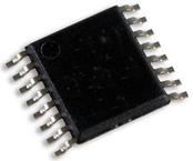
TSSOP-16
描述:
ANALOG DEVICES AD5231BRUZ100 非易失性数字电位器, 100 kohm, 单, SPI, 对数, -40%, +20%, 2.7 V
Pictures:
3D模型
符号图
焊盘图
引脚图
产品图


AD5231BRUZ100数据手册
Page:
of 4 Go
若手册格式错乱,请下载阅览PDF原文件

REV. 0
a
AN-579
APPLICATION NOTE
One Technology Way • P.O. Box 9106 • Norwood, MA 02062-9106 • Tel: 781/329-4700 • Fax: 781/326-8703 • www.analog.com
Versatile Programmable Amplifiers Using
Digital Potentiometers with Nonvolatile Memory
by Alan Li
© 2003 Analog Devices, Inc.
In concept, an op amp and a mechanical potentiometer
can easily be combined to form an adjustable-gain
amplifier, useful in many applications where electronic
adjustments are needed. However, this combination is
often unfeasible because of the potentiometer's limited
resolution, poor temperature coefficient, high resistance
drift over time, and the difficulties of remote adjustment.
Now, the AD523x family of digital potentiometers with
nonvolatile memory* can replace their mechanical
counterparts and make these circuits practical (Figure 1).
CS
SDI
VDD
VSS
CLK
OP1177
+2.7V
–2.7V
–2.7V < V
I
< +2.7V
AB
W
AD5231
V
I
V
O
V+
V–
DIGITAL
INPUTS
U1
A1
GND
C
C
Figure 1. Programmable Amplifier/Attenuator
BASIC PROGRAMMABLE AMPLIFIER
In the circuit of Figure 1, the gain (negative) is simply the
ratio of the two terminal resistances, and the output
voltage is:
V–
R
R
V
O
WB
WA
I
=
×
(1)
V–
D
2–D
V
O
N
I
=
×
(2)
Where:
R
AB
= nominal end-to-end terminal resistance
R
WB
= terminal resistance, W to B,
R
WB
=
R
AB
¥
D
/2
N
R
WA
= terminal resistance, W to A,
RRRR D
WA AB WB AB
N
=- =¥-
()
12
D
= Base-10 equivalent of the binary word
N
= number of bits
The gain expression implies a balanced quasi-logarithmic
characteristic. This inverting configuration is useful
because it makes available a wide range of gains, from
very small to very large, with unity near half-scale.
Because the resistors are fabricated on a single
monolithic chip, resistance ratios are inherently
matched, and the circuit can yield a temperature
coefficient as low as 35 ppm/∞C if using the AD5235.
This circuit is a basic building block that suits many
applications, especially where small signals are present
and where high gain is required. The maximum gain is
limited by the supply voltage. Although the signal is
inverted, the grounded + input minimizes the common-
mode input errors.
Since the potentiometer W terminal parasitic capaci-
tance C
W
(not shown) is connected to the op amp
noninverting node, it introduces a zero for the 1/
O
term
that can lead to 0ⴗ phase margin at the crossover
frequency. The output may ring or oscillate if the input is
a rectangular pulse or step function. Similarly, it is also
likely to ring when switching between two gain values;
this is equivalent to a step change at the input.
As a result, a compensation capacitor C
C
may be added,
as shown, to cancel the effect caused by C
W
. Optimum
compensation occurs when R
WA
⫻ C
W
= R
WB
⫻ C
C
. This is
not an option because of the variation of the resistors.
As a result, C
C
should be found empirically. In general,
C
C
is the range of pFs.
Similarly, there is a B terminal capacitance connected to
the output (not shown). Fortunately, the effect at this
node is less significant and the compensation can be
avoided in most cases.
*The terms “nonvolatile memory” and “E2MEM” are used
interchangeably.
器件 Datasheet 文档搜索
AiEMA 数据库涵盖高达 72,405,303 个元件的数据手册,每天更新 5,000 多个 PDF 文件
