Datasheet 搜索 > DA转换器 > ADI(亚德诺) > AD5381BSTZ-3 数据手册 > AD5381BSTZ-3 用户编程技术手册 1/2 页
 器件3D模型
¥ 7.885
AD5381BSTZ-3 用户编程技术手册 - ADI(亚德诺)
制造商:
ADI(亚德诺)
分类:
DA转换器
封装:
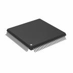
LQFP-100
描述:
ANALOG DEVICES AD5381BSTZ-3 数模转换器, 12 bit, 167 kSPS, 并行、串行, 2.7V 至 3.6V, LQFP, 100 引脚
Pictures:
3D模型
符号图
焊盘图
引脚图
产品图
页面导航:
原理图在P1
导航目录
AD5381BSTZ-3数据手册
Page:
of 2 Go
若手册格式错乱,请下载阅览PDF原文件
AN-1224
APPLICATION NOTE
One Technology Way • P. O. Box 9106 • Norwood, MA 02062-9106, U.S.A. • Tel: 781.329.4700 • Fax: 781.461.3113 • www.analog.com
40 Channels of Programmable Voltage with Excellent Temperature Drift
Performance Using the AD5381 DAC
Rev. B | Page 1 of 2
CIRCUIT FUNCTION AND BENEFITS
This circuit is a multichannel digital-to-analog converter (DAC)
configuration with excellent temperature drift performance. It
provides 40 individual output voltage channels with 12 bits of
resolution and a temperature stability of typically less than
3 ppm/°C.
CIRCUIT DESCRIPTION
Table 1. Devices Connected/Referenced
Product Description
AD5381 40-channel 12-bit 3 V/5 V single-supply DAC
ADR421 Low noise, 2.500 V XFET® voltage references
ADR431 Ultralow noise XFET voltage references
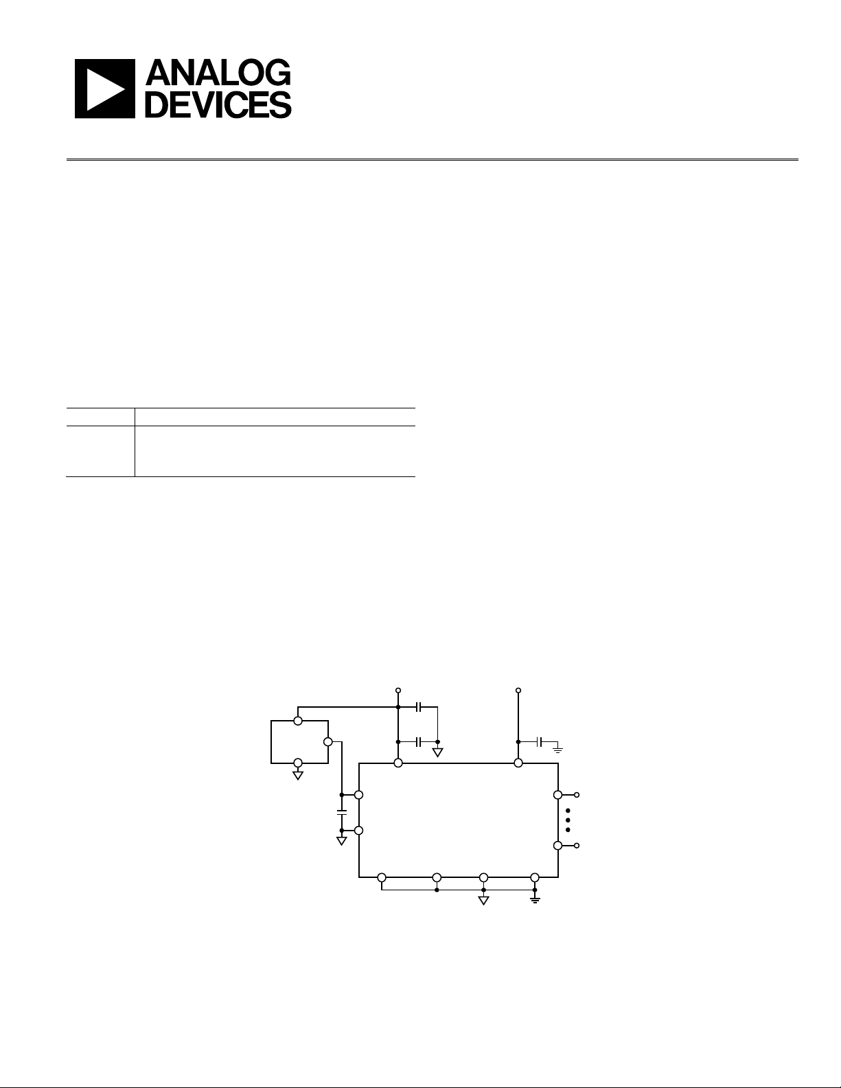
Figure 1 shows a typical configuration for the AD5381 when
configured for use with an external reference. In the circuit
shown, all AGND, SIGNAL_GND, and DAC_GND pins are
tied together to a common AGND. AGND and DGND are
connected together at the AD5381 device. On power-up, the
AD5381 defaults to external reference operation.
This design uses two separate 5.0 V power supplies: one to power
the voltage reference and the analog portion of the AD5381
(AVDD), and the other to power the digital portion of the
AD5381 (DVDD). For best performance, always use a linear
regulator to power the analog portion of the circuit. If a switching
regulator is used to power the digital portion, taken care to
minimize switching noise at the DVDD supply pins. Additional
decoupling using a series connected ferrite bead may be required.
The AD5381 digital (DVDD) power supply can operate from a
3 V or 5 V supply, which provides for maximum flexibility when
interfacing to digital components. Both supplies can be tied
together to a common 5 V supply, provided that supply is derived
from a linear regulator. Refer to the ADIsimPower design tool
for guidance on the power supply designs.
It is recommended to decouple each power pin close to the device
with a 0.1 µF ceramic and a 10 µF tantalum capacitor. In this
circuit, the reference for the AD5380 is provided externally
from either an ADR421 or ADR431 2.5 V reference. The ADR431
provides a lower output voltage noise specification for applications
where that specification is important. Decouple the reference at
the REFOUT/REFIN pin of the device with a 0.1 µF capacitor.
COMMON VARIATIONS
A variation of this circuit uses the AD5381-3 (3 V device) with
the ADR280 1.2 V reference where all other connections and
components are the same as those previously outlined.
08196-001
ADR431/
ADR421
AD5381-5
AVDD
2.5V
5.0V 5.0V
DVDD
SIGNAL_GNDDAC_GND
DGND
VOUT39
VOUT0
AGND
REFOUT/REFIN
REFGND
0.1µF
10µF 0.1µF
0.1µF
Figure 1. AD5381 Typical Configuration with External Reference (Simplified Schematic)
器件 Datasheet 文档搜索
AiEMA 数据库涵盖高达 72,405,303 个元件的数据手册,每天更新 5,000 多个 PDF 文件
