Datasheet 搜索 > AD转换器 > ADI(亚德诺) > AD7191BRUZ 数据手册 > AD7191BRUZ 用户编程技术手册 1/22 页
 器件3D模型
¥ 50.066
AD7191BRUZ 用户编程技术手册 - ADI(亚德诺)
制造商:
ADI(亚德诺)
分类:
AD转换器
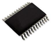
封装:
TSSOP-24
描述:
ANALOG DEVICES AD7191BRUZ. 芯片, 模数转换器, 24位, 120SPS, TSSOP-24
Pictures:
3D模型
符号图
焊盘图
引脚图
产品图
页面导航:
导航目录
AD7191BRUZ数据手册
Page:
of 22 Go
若手册格式错乱,请下载阅览PDF原文件
Pin-Programmable, Ultralow Noise, 24-Bit,
Sigma-Delta ADC for Bridge Sensors
AD7191
Rev. A
Information furnished by Analog Devices is believed to be accurate and reliable. However, no
responsibility is assumed by Analog Devices for its use, nor for any infringements of patents or other
rights of third parties that may result from its use. Specifications subject to change without notice. No
license is granted by implication or otherwise under any patent or patent rights of Analog Devices.
Trademarks and registered trademarks are the property of their respective owners.
One Technology Way, P.O. Box 9106, Norwood, MA 02062-9106, U.S.A.
Tel: 781.329.4700 www.analog.com
Fax: 781.461.3113 ©2009 Analog Devices, Inc. All rights reserved.
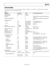
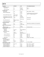
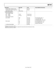
FEATURES
Pin-programmable output rate
Output data rate: 10 Hz, 50 Hz, 60 Hz, 120 Hz
Pin-programmable PGA
Gain: 1, 8, 64, 128
Pin-programmable power-down and reset
RMS noise: 15 nV @ 10 Hz (gain = 128)
Up to 21.5 noise free bits (gain = 1)
Internal or external clock
Bridge power-down switch
Offset drift: 5 nV/°C
Gain drift: 1 ppm/°C
Specified drift over time
Simultaneous 50 Hz/60 Hz rejection
Internal temperature sensor
Power supply: 3 V to 5.25 V
Current: 4.35 mA
Temperature range: –40°C to +105°C
Package: 24-lead TSSOP
INTERFACE
2-wire serial
SPI, QSPI™, and MICROWIRE™ compatible
Schmitt trigger on SCLK
APPLICATIONS
Weigh scales
Strain gauge transducers
Pressure measurement
Medical and scientific instrumentation
GENERAL DESCRIPTION
The AD7191 is a low noise, complete analog front end for high
precision measurement applications. It contains a low noise,
24-bit sigma-delta (Σ-) ADC. The on-chip low noise gain
stage means that signals of small amplitude can be interfaced
directly to the ADC. It contains two differential analog inputs.
The part also includes a temperature sensor that can be used for
temperature compensation.
For ease-of-use, all the features of the AD7191 are controlled by
dedicated pins. The on-chip PGA has a gain of 1, 8, 64, or 128,
supporting a full-scale differential input of ±5 V, ±625 mV,
±78 mV, or ±39 mV. The output data rate can be programmed
to 10 Hz, 50 Hz, 60 Hz, or 120 Hz. Simultaneous 50 Hz and 60 Hz
rejection is obtained when the output data rate is set to 10 Hz
or 50 Hz; 60 Hz only rejection is obtained when the output data
rate is set to 60 Hz. The AD7191 can be operated with the
internal clock, or an external clock can be used.
The part operates with a power supply of 3 V to 5.25 V. It
consumes a current of 4.35 mA. It is available in a 24-lead
TSSOP package.
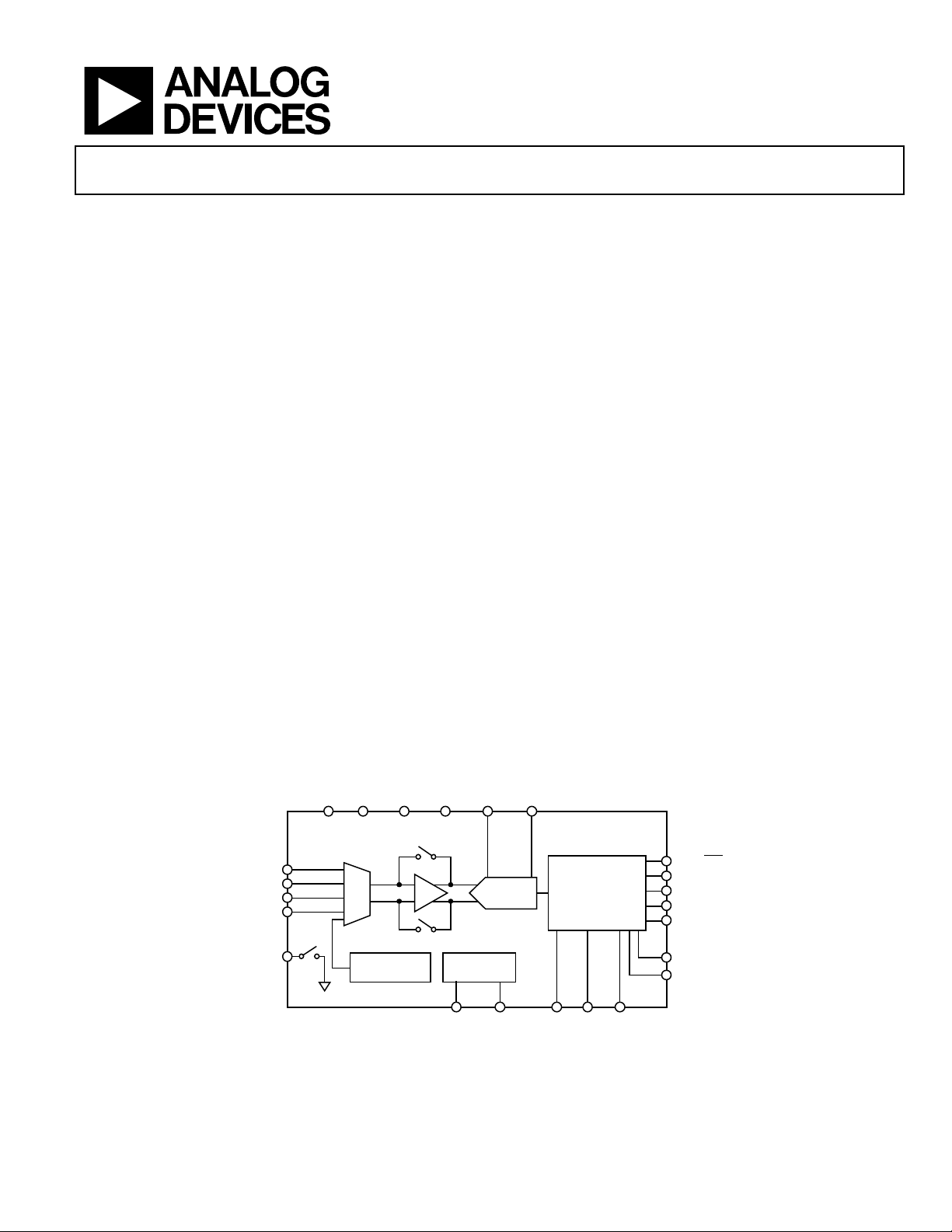
FUNCTIONAL BLOCK DIAGRAM
MUX
AD7191
AIN1
DOUT/RDY
SCLK
PDOWN
CHAN
CLKSEL
PGA2
PGA1
AGND DGND REFIN(+) REFIN(–)
A
V
DD
DV
DD
AIN2
AIN3
AIN4
BPDSW
MCLK1 MCLK2 ODR2 ODR1 TEMP
TEMPERATURE
SENSOR
CLOCK
CIRCUITRY
PGA
SERIAL
INTERFACE
AND CONTROL
LOGIC
Σ-Δ
ADC
08163-001
Figure 1.
器件 Datasheet 文档搜索
AiEMA 数据库涵盖高达 72,405,303 个元件的数据手册,每天更新 5,000 多个 PDF 文件
