Datasheet 搜索 > AD转换器 > ADI(亚德诺) > AD7780BRUZ 数据手册 > AD7780BRUZ 用户编程技术手册 1/18 页

 器件3D模型
¥ 75.573
AD7780BRUZ 用户编程技术手册 - ADI(亚德诺)
制造商:
ADI(亚德诺)
分类:
AD转换器
封装:
TSSOP-16
描述:
ANALOG DEVICES AD7780BRUZ 模数转换器, 24 bit, 16.7 SPS, 单, 2.7 V, 5.25 V, TSSOP
Pictures:
3D模型
符号图
焊盘图
引脚图
产品图
页面导航:
导航目录
AD7780BRUZ数据手册
Page:
of 18 Go
若手册格式错乱,请下载阅览PDF原文件
24-Bit, Pin-Programmable,
Ultralow Power Sigma-Delta ADC
AD7780
Rev. A
Information furnished by Analog Devices is believed to be accurate and reliable. However, no
responsibility is assumed by Analog Devices for its use, nor for any infringements of patents or other
rights of third parties that may result from its use. Specifications subject to change without notice. No
license is granted by implication or otherwise under any patent or patent rights of Analog Devices.
Trademarks and registered trademarks are the property of their respective owners.
One Technology Way, P.O. Box 9106, Norwood, MA 02062-9106, U.S.A.
Tel: 781.329.4700 www.analog.com
Fax: 781.461.3113 ©2009 Analog Devices, Inc. All rights reserved.
FEATURES
Pin-programmable filter response
Update rate: 10 Hz or 16.7 Hz
Pin-programmable in-amp gain
Pin-programmable power-down and reset
Status function
Internal clock oscillator
Internal bridge power-down switch
Current
115 μA typical (gain = 1)
330 μA typical (gain = 128)
Simultaneous 50 Hz/60 Hz rejection
Power supply: 2.7 V to 5.25 V
−40°C to +105°C temperature range
Independent interface power supply
Packages
14-lead, narrow body SOIC
16-lead TSSOP
2-wire serial interface (read-only device)
SPI compatible
Schmitt trigger on SCLK
APPLICATIONS
Weigh scales
Pressure measurement
Industrial process control
Portable instrumentation
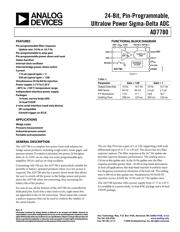
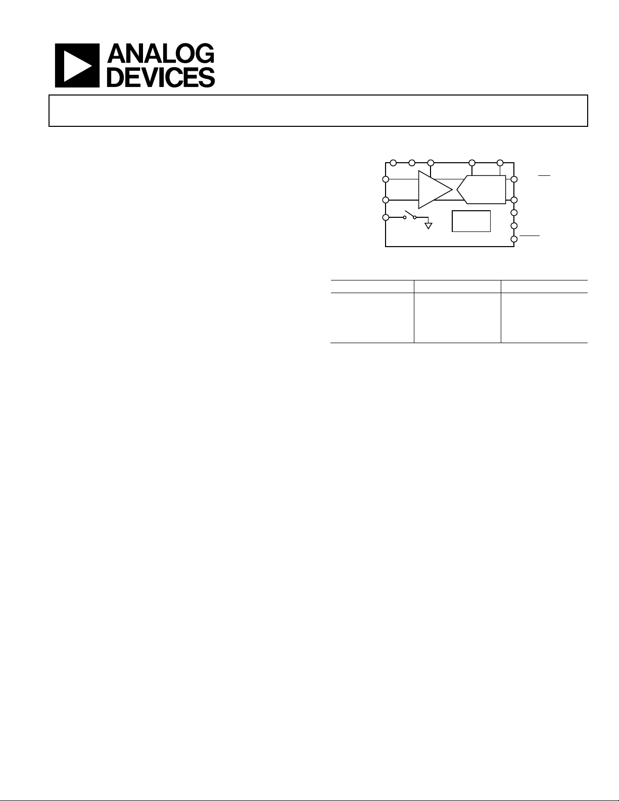
FUNCTIONAL BLOCK DIAGRAM
G = 1
OR 128
24-BIT Σ-Δ
ADC
DOUT/RDY
GND
A
V
DD
AIN(+)
AIN(–) SCLK
DV
DD
FILTER
REFIN(+)GAIN REFIN(–)
INTERNAL
CLOCK
AD7780
PDRST
BPDSW
07945-001
Figure 1.
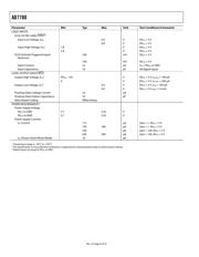
Table 1.
Parameter Gain = 128 Gain = 1
Output Data Rate 10 Hz 16.7 Hz 10 Hz 16.7 Hz
RMS Noise 44 nV 65 nV 2.4 V 2.7 V
P-P Resolution 17.6 17.1 18.8 18.7
Settling Time 300 ms 120 ms 300 ms 120 ms
GENERAL DESCRIPTION
The AD7780 is a complete low power front-end solution for
bridge sensor products, including weigh scales, strain gages, and
pressure sensors. It contains a precision, low power, 24-bit sigma-
delta (Σ-) ADC; an on-chip, low noise programmable gain
amplifier (PGA); and an on-chip oscillator.
Consuming only 330 µA, the AD7780 is particularly suitable for
portable or battery-operated products where very low power is
required. The AD7780 also has a power-down mode that allows
the user to switch off the power to the bridge sensor and power
down the AD7780 when not converting, thus increasing the
battery life of the product.
For ease of use, all the features of the AD7780 are controlled by
dedicated pins. Each time a data read occurs, eight status bits
are appended to the 24-bit conversion. These status bits contain
a pattern sequence that can be used to confirm the validity of
the serial transfer.
The on-chip PGA has a gain of 1 or 128, supporting a full-scale
differential input of ±5 V or ±39 mV. The device has two filter
response options. The filter response at the 16.7 Hz update rate
provides superior dynamic performance. The settling time is
120 ms at this update rate. At the 10 Hz update rate, the filter
response provides greater than −45 dB of stop-band attenuation.
In load cell applications, this stop-band rejection is useful to reject
low frequency mechanical vibrations of the load cell. The settling
time is 300 ms at this update rate. Simultaneous 50 Hz/60 Hz
rejection occurs at both the 10 Hz and 16.7 Hz update rates.
The AD7780 operates with a power supply from 2.7 V to 5.25 V.
It is available in a narrow body, 14-lead SOIC package and a 16-lead
TSSOP package.
器件 Datasheet 文档搜索
AiEMA 数据库涵盖高达 72,405,303 个元件的数据手册,每天更新 5,000 多个 PDF 文件
