Datasheet 搜索 > 开发套件 > ADI(亚德诺) > AD8332-EVALZ 数据手册 > AD8332-EVALZ 用户编程技术手册 2/57 页

¥ 297.227
AD8332-EVALZ 用户编程技术手册 - ADI(亚德诺)
制造商:
ADI(亚德诺)
分类:
开发套件
描述:
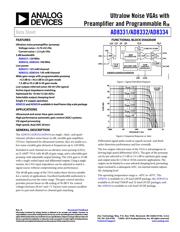
超低噪声可变增益放大器与前置放大器和可编程RIN Ultralow Noise VGAs with Preamplifier and Programmable RIN
Pictures:
3D模型
符号图
焊盘图
引脚图
产品图
页面导航:
引脚图在P8P9P10P54Hot
原理图在P1P24P25P27P28P35P36P37P40P44P49
封装尺寸在P53
型号编码规则在P55
功能描述在P1P8P9P10P39P43P47P54
技术参数、封装参数在P1P4P7
应用领域在P1P26P27P28P29P30P32
电气规格在P12
导航目录
AD8332-EVALZ数据手册
Page:
of 57 Go
若手册格式错乱,请下载阅览PDF原文件

AD8331/AD8332/AD8334 Data Sheet
TABLE OF CONTENTS
Features .............................................................................................. 1
Applications ....................................................................................... 1
General Description ......................................................................... 1
Functional Block Diagram .............................................................. 1
Revision History ............................................................................... 2
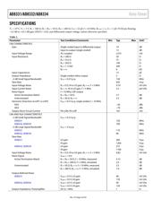
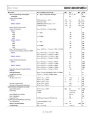
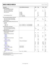
Specifications ..................................................................................... 4
Absolute Maximum Ratings ............................................................ 7
ESD Caution .................................................................................. 7
Pin Configurations and Function Descriptions ........................... 8
Typical Performance Characteristics ........................................... 12
Test Circuits ..................................................................................... 20
Measurement Considerations ................................................... 20
Theory of Operation ...................................................................... 24
Overview ...................................................................................... 24
Low Noise Amplifier (LNA) ..................................................... 25
Variable Gain Amplifier ............................................................ 27
Postamplifier ............................................................................... 28
Applications Information .............................................................. 30
LNA—External Components .................................................... 30
Driving ADCs ............................................................................. 32
Overload ...................................................................................... 32
Optional Input Overload Protection ....................................... 32
Layout, Grounding, and Bypassing .......................................... 33
Multiple Input Matching ........................................................... 33
Disabling the LNA ...................................................................... 33
Ultrasound TGC Application ................................................... 34
High Density Quad Layout ....................................................... 34
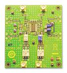
AD8331 Evaluation Board ............................................................ 39
General Description ................................................................... 39
User-Supplied Optional Components ..................................... 39
Measurement Setup.................................................................... 39
Board Layout ............................................................................... 39
AD8331 Evaluation Board Schematics .................................... 40
AD8331 Evaluation Board PCB Layers ................................... 42
AD8332 Evaluation Board ............................................................ 43
General Description ................................................................... 43
User-Supplied Optional Components ..................................... 43
Measurement Setup.................................................................... 43
Board Layout ............................................................................... 43
Evaluation Board Schematics ................................................... 44
AD8332 Evaluation Board PCB Layers ................................... 46
AD8334 Evaluation Board ............................................................ 47
General Description ................................................................... 47
Configuring the Input Impedance ........................................... 48
Measurement Setup.................................................................... 48
Board Layout ............................................................................... 48
Evaluation Board Schematics ................................................... 49
AD8334 Evaluation Board PCB Layers ................................... 51
Outline Dimensions ....................................................................... 53
Ordering Guide .......................................................................... 55
REVISION HISTORY
3/15—Rev. G to Rev. H
Changes to Pin 29 Description; Table 6 ....................................... 11
Updated Figure 123, Figure 124, Figure 125; Outline
Dimensions ...................................................................................... 53
Changes to Ordering Guide .......................................................... 55
10/10—Rev. F to Rev. G
Changes to Quiescent Current per Channel Parameter,
Table 1 ................................................................................................ 6
Changes to Pin 1, Table 3 ................................................................. 8
Changes to Pin 1 and Pin 28, Table 4 and Pin 4 and Pin 5,
Table 5 ................................................................................................ 9
Changes to Figure 6 and Table 6 ................................................... 10
Changes to Figure 33 ...................................................................... 16
Changes to Figure 64 ...................................................................... 22
Changes to Figure 70 ...................................................................... 24
Changes to Low Noise Amplifier (LNA) Section and
Figure 74 .......................................................................................... 25
Changes to Figure 94 ...................................................................... 38
Changes to General Descriptions Section, Figure 95 Caption,
Table 10, and Board Layout Section ............................................. 39
Changes to Figure 96 ...................................................................... 40
Changes to Figure 97 ...................................................................... 41
Changes to Figure 98 and Figure 103 .......................................... 42
Deleted AD8331 Bill of Materials Section and Table 11;
Renumbered Sequentially ............................................................. 43
Changes to Figure 104 ................................................................... 43
Changes to Figure 106 ................................................................... 45
Changes to Figure 107 ................................................................... 46
Changes to Figure 113 ................................................................... 47
Changes to Figure 114 and Board Layout Section ..................... 48
Deleted AD8332 Bill of Materials Section and Table 13;
Renumbered Sequentially ............................................................. 48
Rev. H | Page 2 of 56
器件 Datasheet 文档搜索
AiEMA 数据库涵盖高达 72,405,303 个元件的数据手册,每天更新 5,000 多个 PDF 文件
