Datasheet 搜索 > 放大器、缓冲器 > ADI(亚德诺) > AD8336ACPZ-R7 数据手册 > AD8336ACPZ-R7 用户编程技术手册 1/28 页
 器件3D模型
¥ 28.842
AD8336ACPZ-R7 用户编程技术手册 - ADI(亚德诺)
制造商:
ADI(亚德诺)
分类:
放大器、缓冲器
封装:
LFCSP-16
描述:
ANALOG DEVICES AD8336ACPZ-R7 芯片, 可变增益放大器, 150MHZ, LFCSP-16
Pictures:
3D模型
符号图
焊盘图
引脚图
产品图
页面导航:
导航目录
AD8336ACPZ-R7数据手册
Page:
of 28 Go
若手册格式错乱,请下载阅览PDF原文件
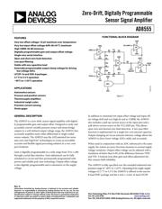
Zero-Drift, Digitally Programmable
Sensor Signal Amplifier
AD8555
Rev. A
Information furnished by Analog Devices is believed to be accurate and reliable.
However, no responsibility is assumed by Analog Devices for its use, nor for any
infringements of patents or other rights of third parties that may result from its use.
Specifications subject to change without notice. No license is granted by implication
or otherwise under any patent or patent rights of Analog Devices. Trademarks and
registered trademarks are the property of their respective owners.
One Technology Way, P.O. Box 9106, Norwood, MA 02062-9106, U.S.A.
Tel: 781.329.4700 www.analog.com
Fax: 781.326.8703©2004–2009 Analog Devices, Inc. All rights reserved.
FEATURES
Very low offset voltage: 10 μV maximum over temperature
Very low input offset voltage drift: 60 nV/°C maximum
High CMRR: 96 dB minimum
Digitally programmable gain and output offset voltage
Single-wire serial interface
Open and short wire fault detection
Low-pass filtering
Stable with any capacitive load
Externally programmable output clamp voltage for driving
low voltage ADCs
LFCSP-16 and SOIC-8 packages
2.7 V to 5.5 V operation
−40°C to +125°C operation
APPLICATIONS
Automotive sensors
Pressure and position sensors
Thermocouple amplifiers
Industrial weigh scales
Precision current sensing
Strain gages
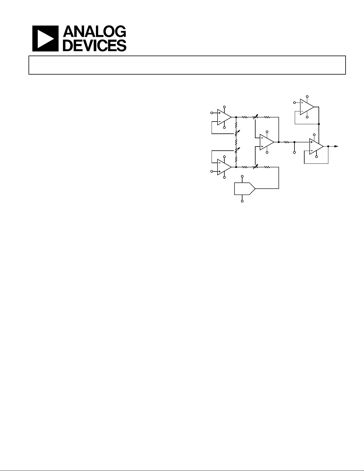
FUNCTIONAL BLOCK DIAGRAM
A3
A2
A4
A5
VDD
VDD
DAC
VSS
VSS
VDD
VSS
VDD
VDD
VSS
VCLAMP
VPOS
VSS
FILT/
DIGOUT
VOUT
A1
VDD
VSS
V
NEG
R1
R3
R2
R5 R7
P4
R4
R6
RF
P3
P2
P1
04598-0-001
Figure 1.
GENERAL DESCRIPTION
The AD8555 is a zero-drift, sensor signal amplifier with digital-
ly programmable gain and output offset. Designed to easily and
accurately convert variable pressure sensor and strain bridge
outputs to a well-defined output voltage range, the AD8555 also
accurately amplifies many other differential or single-ended
sensor outputs. The AD8555 uses the ADI patented low noise
auto-zero and DigiTrim® technologies to create an incredibly
accurate and flexible signal processing solution in a very com-
pact footprint.
Gain is digitally programmable in a wide range from 70 to 1,280
through a serial data interface. Gain adjustment can be fully
simulated in-circuit and then permanently programmed with
proven and reliable poly-fuse technology. Output offset voltage
is also digitally programmable and is ratiometric to the supply
voltage.
In addition to extremely low input offset voltage and input off-
set voltage drift and very high dc and ac CMRR, the AD8555
also includes a pull-up current source at the input pins and a
pull-down current source at the VCLAMP pin. This allows
open wire and shorted wire fault detection. A low-pass filter
function is implemented via a single low cost external capacitor.
Output clamping set via an external reference voltage allows the
AD8555 to drive lower voltage ADCs safely and accurately.
When used in conjunction with an ADC referenced to the same
supply, the system accuracy becomes immune to normal supply
voltage variations. Output offset voltage can be adjusted with a
resolution of better than 0.4% of the difference between VDD
and VSS. A lockout trim after gain and offset adjustment fur-
ther ensures field reliability.
The AD8555 is fully specified over the extended industrial tem-
perature range of −40°C to +125°C. Operating from single-supply
voltages of 2.7 V to 5.5 V, the AD8555 is offered in the narrow
8-lead SOIC package and the 4 mm × 4 mm 16-lead LFCSP.
器件 Datasheet 文档搜索
AiEMA 数据库涵盖高达 72,405,303 个元件的数据手册,每天更新 5,000 多个 PDF 文件
