Datasheet 搜索 > 运算放大器 > ADI(亚德诺) > ADA4500-2ARMZ-R7 数据手册 > ADA4500-2ARMZ-R7 用户编程技术手册 1/2 页
 器件3D模型
¥ 19.154
ADA4500-2ARMZ-R7 用户编程技术手册 - ADI(亚德诺)
制造商:
ADI(亚德诺)
分类:
运算放大器
封装:
MSOP-8
描述:
10兆赫, 14.5纳伏/ A ????赫兹,轨至轨I / O,零输入交越失真放大器 10 MHz, 14.5 nV/âHz, Rail-to-Rail I/O, Zero Input Crossover Distortion Amplifier
Pictures:
3D模型
符号图
焊盘图
引脚图
产品图


ADA4500-2ARMZ-R7数据手册
Page:
of 2 Go
若手册格式错乱,请下载阅览PDF原文件
A Relatively Easy Way to Realize a
Programmable LED Driver
Thomas Brand
Analog Devices, Inc.
LEDs are increasingly being used as energy saving light sources as a
response to new energy regulations. They have decisive advantages over
conventional lights: they consume less energy, have longer lifetimes, and
are available in various colors. For example, thanks to LEDs, the largest
church in the world, St. Peter’s Basilica in Rome, can now be seen in a
new light. Via an intelligent control system, even the smallest details of
its important treasures can be illuminated with preset lighting scenarios.
These digitally controlled systems integrate programmable LED drivers,
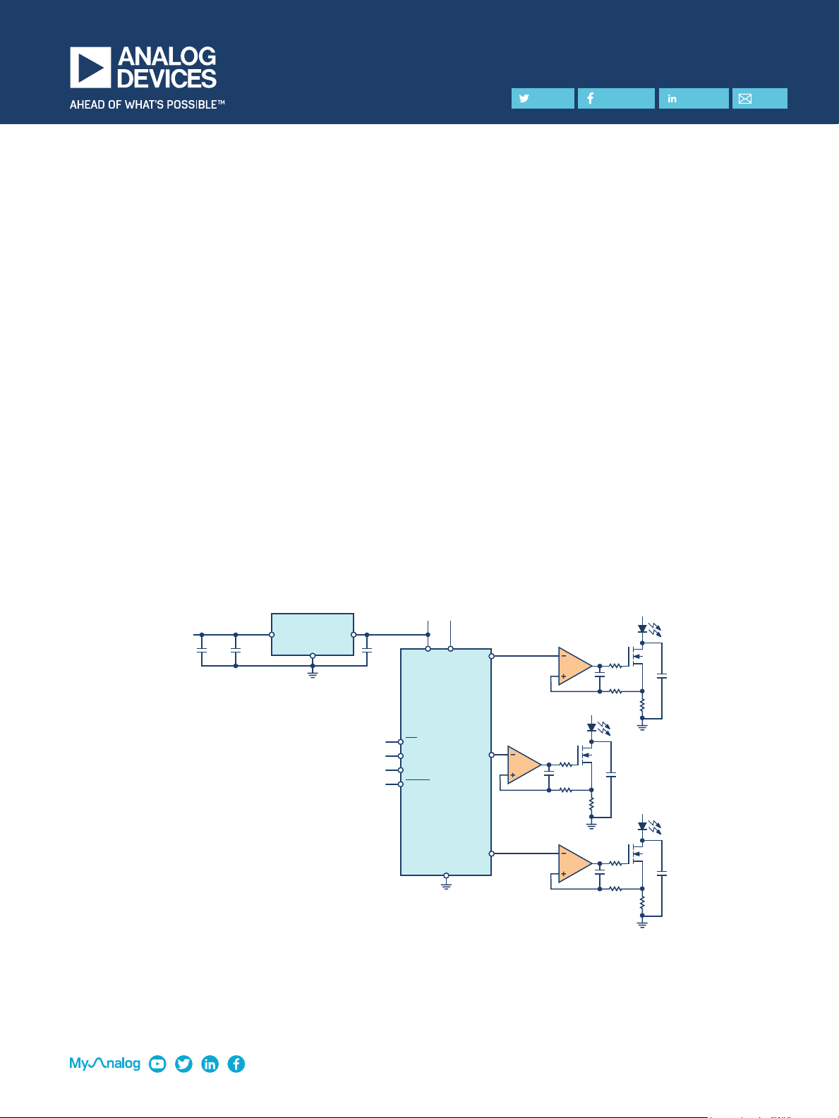
with which the LEDs can be activated as desired. Figure 1 shows an
example of a 3-channel LED driver configuration.
Each of the three output voltages of the digital-to-analog converter
(
DAC
)
,
in this case the AD5686 from Analog Devices, Inc.
(
ADI
)
, controls
a voltage-to-current converter stage in whose load path the individual
LED is situated for each LED channel. All three converter stages are
realized by an operational amplifier
(
op amp
)
, ADA4500-2, and a con-
nected MOSFET, which controls the LED current. This LED current can
theoretically be up to several amps, depending on the voltage source
(
VS
)
and the load resistance, which is 2 Ω in this circuit. Thus, the
selection of a suitable MOSFET is very important.
The quality of the DAC output voltages is strongly dependent on the
reference voltage source V
REF
. A high quality reference source should
be used. The ADR4520 is one such example, as shown in Figure1. It
offers very low noise, extremely high and long-term accuracy, and high
temperature stability.
Due to ADR4500-2’s internal design, typical rail-to-rail amplifiers exhibit
a certain nonlinearity and crossover distortion. Their input stage consists
of two differential transistors connected in parallel: a PNP stage
(
Q1and
Q2
)
and an NPN stage
(
Q3 and Q4
)
, as shown in Figure 2.
ADA4500-2
VS
VS
VS
1 kΩ
1 kΩ
1 nF
1 µF0.1 µF1 µF
2 µ
F
2 Ω
LED
V
OUTA
ADA4500-2
1 kΩ
1 kΩ
1 nF
2 µ
F
2 Ω
LED
V
OUTC
ADA4500-2
1 kΩ
1 kΩ
1 nF
2 µF
2 Ω
LED
V
OUTB
OUT
OUT
IN
V
REF
VDD
3.3 V
V
REF
3.3 V
CS
SYNC
GND1
AD5686
ADR4520
SCLK
MOSI
Figure 1. Simplified schematic of an LED driver for control of three separate LEDs.
Visit analog.com
Technical Article
Share on
Twitter LinkedIn Facebook Email
器件 Datasheet 文档搜索
AiEMA 数据库涵盖高达 72,405,303 个元件的数据手册,每天更新 5,000 多个 PDF 文件
