Datasheet 搜索 > 微控制器 > Microchip(微芯) > AT89C5130A-S3SUM 数据手册 > AT89C5130A-S3SUM 用户编程技术手册 3/3 页

 器件3D模型
¥ 19.009
AT89C5130A-S3SUM 用户编程技术手册 - Microchip(微芯)
制造商:
Microchip(微芯)
分类:
微控制器
封装:
PLCC-52
Pictures:
3D模型
符号图
焊盘图
引脚图
产品图
AT89C5130A-S3SUM数据手册
Page:
of 3 Go
若手册格式错乱,请下载阅览PDF原文件
3
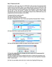
Step 3: Program and verify
By default (e.g. with a new chip), the AT89C51RC2 starts execution from the boot loader
location and not from 0000h. Hence, if you replace the C501 with the AT89C51RC2 and
expect to execute code from external memory location 0000h (assuming /EA is low), it will
not quite work that way and will instead jump to the bootloader. In order make the Atmel
part act like a C501 and execute a program from external memory location 0000h
automatically after reset, the Boot Loader Jump Bit (BLJB) of the AT89C51RC2 has to be
programmed such that reset address is set at 0000h.
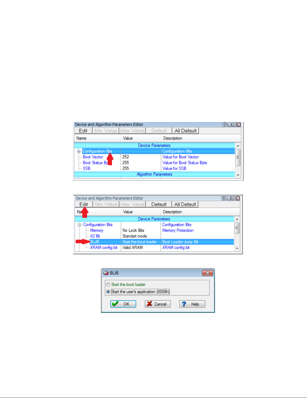
To program the Boot Loader Jump Bit:
Click on Select Device option
Select the correct device (AT89C51RC2)
Select “Configuration Bits” from “Device and Algorithms Parameter Editor” Window.
Select BLJB (Boot Loader Jump Bit) and click “Edit”.
Select the start address as 0000h. By default, the boot loader is selected.
Since the configuration bit is changed, the device needs to be re-programmed for
changes to come into effect.
Note: By default, the XRAM is enabled for the device. If desired, this parameter can be
changed by modifying the “XRAM Config bit” from the “Device and Algorithms Parameter
Editor” window above.
Note: For more details, refer to the User’s Guide in the ChipProgUSB Help menu.
器件 Datasheet 文档搜索
AiEMA 数据库涵盖高达 72,405,303 个元件的数据手册,每天更新 5,000 多个 PDF 文件
