Datasheet 搜索 > 微控制器 > Microchip(微芯) > ATMEGA128-16ANR 数据手册 > ATMEGA128-16ANR 用户编程技术手册 4/386 页
 器件3D模型
¥ 35.75
ATMEGA128-16ANR 用户编程技术手册 - Microchip(微芯)
制造商:
Microchip(微芯)
分类:
微控制器
封装:
TQFP-64
Pictures:
3D模型
符号图
焊盘图
引脚图
产品图
页面导航:
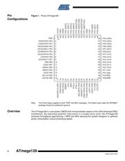
引脚图在P2P5P68P93P112P146Hot
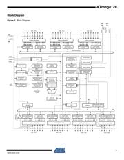
原理图在P3P10P66P93P94P96P97P113P118P119P121P123
封装尺寸在P369P370
型号编码规则在P368P374P375P376P378
封装信息在P369P376
应用领域在P34P50P61P64P273P276P284P286P287
电气规格在P90P375


导航目录
ATMEGA128-16ANR数据手册
Page:
of 386 Go
若手册格式错乱,请下载阅览PDF原文件

4
2467S–AVR–07/09
ATmega128
The AVR core combines a rich instruction set with 32 general purpose working registers. All the
32 registers are directly connected to the Arithmetic Logic Unit (ALU), allowing two independent
registers to be accessed in one single instruction executed in one clock cycle. The resulting
architecture is more code efficient while achieving throughputs up to ten times faster than con-
ventional CISC microcontrollers.
The ATmega128 provides the following features: 128K bytes of In-System Programmable Flash
with Read-While-Write capabilities, 4K bytes EEPROM, 4K bytes SRAM, 53 general purpose I/O
lines, 32 general purpose working registers, Real Time Counter (RTC), four flexible Timer/Coun-
ters with compare modes and PWM, 2 USARTs, a byte oriented Two-wire Serial Interface, an 8-
channel, 10-bit ADC with optional differential input stage with programmable gain, programma-
ble Watchdog Timer with Internal Oscillator, an SPI serial port, IEEE std. 1149.1 compliant
JTAG test interface, also used for accessing the On-chip Debug system and programming and
six software selectable power saving modes. The Idle mode stops the CPU while allowing the
SRAM, Timer/Counters, SPI port, and interrupt system to continue functioning. The Power-down
mode saves the register contents but freezes the Oscillator, disabling all other chip functions
until the next interrupt or Hardware Reset. In Power-save mode, the asynchronous timer contin-
ues to run, allowing the user to maintain a timer base while the rest of the device is sleeping.
The ADC Noise Reduction mode stops the CPU and all I/O modules except Asynchronous
Timer and ADC, to minimize switching noise during ADC conversions. In Standby mode, the
Crystal/Resonator Oscillator is running while the rest of the device is sleeping. This allows very
fast start-up combined with low power consumption. In Extended Standby mode, both the main
Oscillator and the Asynchronous Timer continue to run.
The device is manufactured using Atmel’s high-density nonvolatile memory technology. The On-
chip ISP Flash allows the program memory to be reprogrammed in-system through an SPI serial
interface, by a conventional nonvolatile memory programmer, or by an On-chip Boot program
running on the AVR core. The boot program can use any interface to download the application
program in the application Flash memory. Software in the Boot Flash section will continue to run
while the Application Flash section is updated, providing true Read-While-Write operation. By
combining an 8-bit RISC CPU with In-System Self-Programmable Flash on a monolithic chip,
the Atmel ATmega128 is a powerful microcontroller that provides a highly flexible and cost effec-
tive solution to many embedded control applications.
The ATmega128 AVR is supported with a full suite of program and system development tools
including: C compilers, macro assemblers, program debugger/simulators, in-circuit emulators,
and evaluation kits.
ATmega103 and
ATmega128
Compatibility
The ATmega128 is a highly complex microcontroller where the number of I/O locations super-
sedes the 64 I/O locations reserved in the AVR instruction set. To ensure backward compatibility
with the ATmega103, all I/O locations present in ATmega103 have the same location in
ATmega128. Most additional I/O locations are added in an Extended I/O space starting from $60
to $FF, (i.e., in the ATmega103 internal RAM space). These locations can be reached by using
LD/LDS/LDD and ST/STS/STD instructions only, not by using IN and OUT instructions. The relo-
cation of the internal RAM space may still be a problem for ATmega103 users. Also, the
increased number of interrupt vectors might be a problem if the code uses absolute addresses.
To solve these problems, an ATmega103 compatibility mode can be selected by programming
the fuse M103C. In this mode, none of the functions in the Extended I/O space are in use, so the
internal RAM is located as in ATmega103. Also, the Extended Interrupt vectors are removed.
The ATmega128 is 100% pin compatible with ATmega103, and can replace the ATmega103 on
current Printed Circuit Boards. The application note “Replacing ATmega103 by ATmega128”
describes what the user should be aware of replacing the ATmega103 by an ATmega128.
器件 Datasheet 文档搜索
AiEMA 数据库涵盖高达 72,405,303 个元件的数据手册,每天更新 5,000 多个 PDF 文件
