Datasheet 搜索 > RF射频器件 > ATMEL(爱特美尔) > ATMEGA128RFA1-ZUR 数据手册 > ATMEGA128RFA1-ZUR 用户编程技术手册 6/570 页
 器件3D模型
¥ 47.985
ATMEGA128RFA1-ZUR 用户编程技术手册 - ATMEL(爱特美尔)
制造商:
ATMEL(爱特美尔)
分类:
RF射频器件
封装:
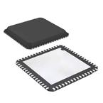
QFN-64
Pictures:
3D模型
符号图
焊盘图
引脚图
产品图
页面导航:
引脚图在P2P5P192P229P247P312P560Hot
典型应用电路图在P82P155P500
原理图在P3P9P31P43P76P78P81P83P91P168P190P229
型号编码规则在P552
封装信息在P553
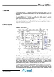
功能描述在P63P334
技术参数、封装参数在P77P90P102P512P523P525
应用领域在P1P92P157P180P216P220P455P470P471P500P502P514
电气规格在P73P156P166P178P179P190P207P208P416P418P512P516
导航目录
ATMEGA128RFA1-ZUR数据手册
Page:
of 570 Go
若手册格式错乱,请下载阅览PDF原文件

6
8266F-MCU Wireless-09/14
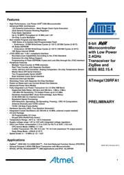
ATmega128RFA1
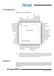
Port E also provides functions of various special features of the ATmega128RFA1.
3.2.10 Port F (PF7...PF0)
Port F is an 8-bit bi-directional I/O port with internal pull-up resistors (selected for each
bit). The Port F output buffers have symmetrical drive characteristics with both high sink
and source capability. As inputs, Port F pins that are externally pulled low will source
current if the pull-up resistors are activated. The Port F pins are tri-stated when a reset
condition becomes active, even if the clock is not running.
Port F also provides functions of various special features of the ATmega128RFA1.
3.2.11 Port G (PG5…PG0)
Port G is a 6-bit bi-directional I/O port with internal pull-up resistors (selected for each
bit). The Port G output buffers have symmetrical drive characteristics with both high
sink and source capability. However the driver strength of PG3 and PG4 is reduced
compared to the other port pins. The output voltage drop (V
OH
, V
OL
) is higher while the
leakage current is smaller. As inputs, Port G pins that are externally pulled low will
source current if the pull-up resistors are activated. The Port G pins are tri-stated when
a reset condition becomes active, even if the clock is not running.
Port G also provides functions of various special features of the ATmega128RFA1.
3.2.12 AVSS_RFP
AVSS_RFP is a dedicated ground pin for the bi-directional, differential RF I/O port.
3.2.13 AVSS_RFN
AVSS_RFN is a dedicated ground pin for the bi-directional, differential RF I/O port.
3.2.14 RFP
RFP is the positive terminal for the bi-directional, differential RF I/O port.
3.2.15 RFN
RFN is the negative terminal for the bi-directional, differential RF I/O port.
3.2.16 RSTN
Reset input. A low level on this pin for longer than the minimum pulse length will
generate a reset, even if the clock is not running. Shorter pulses are not guaranteed to
generate a reset.
3.2.17 RSTON
Reset output. A low level on this pin indicates a reset initiated by the internal reset
sources or the pin RSTN.
3.2.18 XTAL1
Input to the inverting 16MHz crystal oscillator amplifier. In general a crystal between
XTAL1 and XTAL2 provides the 16MHz reference clock of the radio transceiver.
3.2.19 XTAL2
Output of the inverting 16MHz crystal oscillator amplifier.
3.2.20 AREF
Reference voltage output of the A/D Converter. In general this pin is left open.
3.2.21 TST
Programming and test mode enable pin. If pin TST is not used pull it to low.
3.2.22 CLKI
Input to the clock system. If selected, it provides the operating clock of the
microcontroller.
器件 Datasheet 文档搜索
AiEMA 数据库涵盖高达 72,405,303 个元件的数据手册,每天更新 5,000 多个 PDF 文件
