Datasheet 搜索 > 微控制器 > Microchip(微芯) > ATMEGA328P-MN 数据手册 > ATMEGA328P-MN 用户编程技术手册 4/661 页
 器件3D模型
¥ 26.075
ATMEGA328P-MN 用户编程技术手册 - Microchip(微芯)
制造商:
Microchip(微芯)
分类:
微控制器
封装:
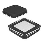
VQFN-32
描述:
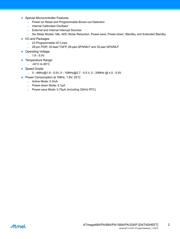
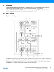
ATmega328P 8 位 megaAVR picoPower 微控制器Atmel ATmega328P 微控制器是基于 AVR 增强型 RISC 体系架构的 8 位 megaAVR 设备。 其特色为 picoPower 技术,可提供超低功耗和低功率睡眠模式,非常适合用于电池供电型应用。### 微控制器功能20 MHz 最大工作频率 20 MHz 时高达 20 MIPS 32 KB 闪存 1024 B EEPROM 2 KB SRAM 131 指令 – 大多数单一时钟周期执行 32 个通用寄存器 23 GPIO 通电重置和可编程掉电检测 内部校准振荡器 外部和内部中断源 六个省电睡眠模式 内部和外部中断 完全静态操作### 外围功能10 位 15 ksps 模拟至数字转换器 (ADC) - 8 或 6 通道 电容性触摸传感 - 16 通道 温度传感器 两个 8 位计时器 一个 16 位计时器 输出比较模块 - 6 通道 六个 PWM 通道 可编程串行 USART 主/从 SPI 串行接口 面向字节的 2 线串行接口 – I2C 兼容 可编程监看计时器,带单独振荡器 模拟比较器 引脚变化时的中断和唤醒
Pictures:
3D模型
符号图
焊盘图
引脚图
产品图
页面导航:
引脚图在P3P4P77Hot
原理图在P6P9P75P93P95P96P97P112P117P118P120P121
封装尺寸在P627P628P629P630P631P649
型号编码规则在P619P620P621P622P623P624P625P626P649
封装信息在P627P649P650
技术参数、封装参数在P299P313
应用领域在P37P47P59P63P66P68P263P267P281P660
电气规格在P75P253P299P313P649
导航目录
ATMEGA328P-MN数据手册
Page:
of 661 Go
若手册格式错乱,请下载阅览PDF原文件

4
ATmega48A/PA/88A/PA/168A/PA/328/P [DATASHEET]
Atmel-8271J-AVR- ATmega-Datasheet_11/2015
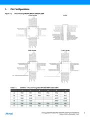
1.1 Pin Descriptions
1.1.1 VCC
Digital supply voltage.
1.1.2 GND
Ground.
1.1.3 Port B (PB7:0) XTAL1/XTAL2/TOSC1/TOSC2
Port B is an 8-bit bi-directional I/O port with internal pull-up resistors (selected for each bit). The Port B output
buffers have symmetrical drive characteristics with both high sink and source capability. As inputs, Port B pins
that are externally pulled low will source current if the pull-up resistors are activated. The Port B pins are tri-
stated when a reset condition becomes active, even if the clock is not running.
Depending on the clock selection fuse settings, PB6 can be used as input to the inverting Oscillator amplifier
and input to the internal clock operating circuit.
Depending on the clock selection fuse settings, PB7 can be used as output from the inverting Oscillator
amplifier.
If the Internal Calibrated RC Oscillator is used as chip clock source, PB7...6 is used as TOSC2...1 input for the
Asynchronous Timer/Counter2 if the AS2 bit in ASSR is set.
The various special features of Port B are elaborated in ”Alternate Functions of Port B” on page 82 and ”System
Clock and Clock Options” on page 27.
1.1.4 Port C (PC5:0)
Port C is a 7-bit bi-directional I/O port with internal pull-up resistors (selected for each bit). The PC5...0 output
buffers have symmetrical drive characteristics with both high sink and source capability. As inputs, Port C pins
that are externally pulled low will source current if the pull-up resistors are activated. The Port C pins are tri-
stated when a reset condition becomes active, even if the clock is not running.
1.1.5 PC6/RESET
If the RSTDISBL Fuse is programmed, PC6 is used as an I/O pin. Note that the electrical characteristics of PC6
differ from those of the other pins of Port C.
If the RSTDISBL Fuse is unprogrammed, PC6 is used as a Reset input. A low level on this pin for longer than
the minimum pulse length will generate a Reset, even if the clock is not running. The minimum pulse length is
given in Table 29-11 on page 305. Shorter pulses are not guaranteed to generate a Reset.
The various special features of Port C are elaborated in ”Alternate Functions of Port C” on page 85.|
1.1.6 Port D (PD7:0)
Port D is an 8-bit bi-directional I/O port with internal pull-up resistors (selected for each bit). The Port D output
buffers have symmetrical drive characteristics with both high sink and source capability. As inputs, Port D pins
that are externally pulled low will source current if the pull-up resistors are activated. The Port D pins are tri-
stated when a reset condition becomes active, even if the clock is not running.
The various special features of Port D are elaborated in ”Alternate Functions of Port D” on page 88.
器件 Datasheet 文档搜索
AiEMA 数据库涵盖高达 72,405,303 个元件的数据手册,每天更新 5,000 多个 PDF 文件
