Datasheet 搜索 > 8位微控制器 > Microchip(微芯) > ATMEGA328P-MUR 数据手册 > ATMEGA328P-MUR 用户编程技术手册 4/51 页
 器件3D模型
¥ 9.535
ATMEGA328P-MUR 用户编程技术手册 - Microchip(微芯)
制造商:
Microchip(微芯)
分类:
8位微控制器
封装:
QFN-32
描述:
8位 MCU微控制单元, 低功率高性能, AVR ATmega Family ATmega328 Series Microcontrollers, 20 MHz, 32 KB, 2 KB
Pictures:
3D模型
符号图
焊盘图
引脚图
产品图
页面导航:
引脚图在P3P4Hot
原理图在P6
封装尺寸在P24P25P26P27P28P48
型号编码规则在P16P17P18P19P20P21P22P23P48
封装信息在P24P48P49
应用领域在P50
电气规格在P48
导航目录
ATMEGA328P-MUR数据手册
Page:
of 51 Go
若手册格式错乱,请下载阅览PDF原文件

4
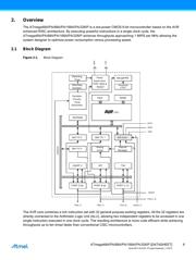
ATmega48A/PA/88A/PA/168A/PA/328/P [DATASHEET]
Atmel-8271JS-AVR- ATmega-Datasheet_11/2015
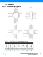
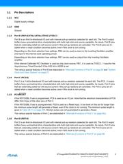
1.1 Pin Descriptions
1.1.1 VCC
Digital supply voltage.
1.1.2 GND
Ground.
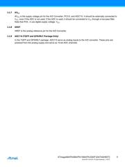
1.1.3 Port B (PB7:0) XTAL1/XTAL2/TOSC1/TOSC2
Port B is an 8-bit bi-directional I/O port with internal pull-up resistors (selected for each bit). The Port B output
buffers have symmetrical drive characteristics with both high sink and source capability. As inputs, Port B pins
that are externally pulled low will source current if the pull-up resistors are activated. The Port B pins are tri-
stated when a reset condition becomes active, even if the clock is not running.
Depending on the clock selection fuse settings, PB6 can be used as input to the inverting Oscillator amplifier
and input to the internal clock operating circuit.
Depending on the clock selection fuse settings, PB7 can be used as output from the inverting Oscillator
amplifier.
If the Internal Calibrated RC Oscillator is used as chip clock source, PB7...6 is used as TOSC2...1 input for the
Asynchronous Timer/Counter2 if the AS2 bit in ASSR is set.
The various special features of Port B are elaborated in ”Alternate Functions of Port B” on page 82 and ”System
Clock and Clock Options” on page 27.
1.1.4 Port C (PC5:0)
Port C is a 7-bit bi-directional I/O port with internal pull-up resistors (selected for each bit). The PC5...0 output
buffers have symmetrical drive characteristics with both high sink and source capability. As inputs, Port C pins
that are externally pulled low will source current if the pull-up resistors are activated. The Port C pins are tri-
stated when a reset condition becomes active, even if the clock is not running.
1.1.5 PC6/RESET
If the RSTDISBL Fuse is programmed, PC6 is used as an I/O pin. Note that the electrical characteristics of PC6
differ from those of the other pins of Port C.
If the RSTDISBL Fuse is unprogrammed, PC6 is used as a Reset input. A low level on this pin for longer than
the minimum pulse length will generate a Reset, even if the clock is not running. The minimum pulse length is
given in Table 29-11 on page 305. Shorter pulses are not guaranteed to generate a Reset.
The various special features of Port C are elaborated in ”Alternate Functions of Port C” on page 85.|
1.1.6 Port D (PD7:0)
Port D is an 8-bit bi-directional I/O port with internal pull-up resistors (selected for each bit). The Port D output
buffers have symmetrical drive characteristics with both high sink and source capability. As inputs, Port D pins
that are externally pulled low will source current if the pull-up resistors are activated. The Port D pins are tri-
stated when a reset condition becomes active, even if the clock is not running.
The various special features of Port D are elaborated in ”Alternate Functions of Port D” on page 88.
器件 Datasheet 文档搜索
AiEMA 数据库涵盖高达 72,405,303 个元件的数据手册,每天更新 5,000 多个 PDF 文件
