Datasheet 搜索 > 8位微控制器 > Microchip(微芯) > ATMEGA88A-AU 数据手册 > ATMEGA88A-AU 用户编程技术手册 4/40 页
 器件3D模型
¥ 13.031
ATMEGA88A-AU 用户编程技术手册 - Microchip(微芯)
制造商:
Microchip(微芯)
分类:
8位微控制器
封装:
TQFP-32
描述:
8 位 megaAVR 微控制器,4KB 到 16KB 闪存我们在 RS Components 提供 Atmel 的各种 megaAVR 8 位微控制器。每个微控制器均基于增强型 RISC 体系结构,并具有 QTouch 库支持。 所有 megaAVR 微控制器具有不同 Kb 的系统内可编程内存、EEPROM 和 SRAM 以及不同引脚和封装类型。 **megaAVR 8 位微控制器类型 ** ATmega8 ATmega16 ATmega48 ATmega88 ATmega162 ATmega164 ATmega165 ATmega168 ATmega8515 ATmega8535
Pictures:
3D模型
符号图
焊盘图
引脚图
产品图
页面导航:

导航目录
ATMEGA88A-AU数据手册
Page:
of 40 Go
若手册格式错乱,请下载阅览PDF原文件

4
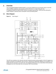
ATmega48A/PA/88A/PA/168A/PA/328/P [DATASHEET]
Atmel-8271IS-AVR- ATmega-Datasheet_10/2014
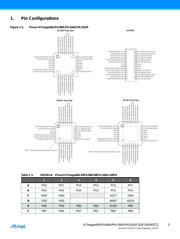
1.1 Pin Descriptions
1.1.1 VCC
Digital supply voltage.
1.1.2 GND
Ground.
1.1.3 Port B (PB7:0) XTAL1/XTAL2/TOSC1/TOSC2
Port B is an 8-bit bi-directional I/O port with internal pull-up resistors (selected for each bit). The Port B output
buffers have symmetrical drive characteristics with both high sink and source capability. As inputs, Port B pins
that are externally pulled low will source current if the pull-up resistors are activated. The Port B pins are tri-
stated when a reset condition becomes active, even if the clock is not running.
Depending on the clock selection fuse settings, PB6 can be used as input to the inverting Oscillator amplifier
and input to the internal clock operating circuit.
Depending on the clock selection fuse settings, PB7 can be used as output from the inverting Oscillator
amplifier.
If the Internal Calibrated RC Oscillator is used as chip clock source, PB7...6 is used as TOSC2...1 input for the
Asynchronous Timer/Counter2 if the AS2 bit in ASSR is set.
The various special features of Port B are elaborated in ”Alternate Functions of Port B” on page 82 and ”System
Clock and Clock Options” on page 27.
1.1.4 Port C (PC5:0)
Port C is a 7-bit bi-directional I/O port with internal pull-up resistors (selected for each bit). The PC5...0 output
buffers have symmetrical drive characteristics with both high sink and source capability. As inputs, Port C pins
that are externally pulled low will source current if the pull-up resistors are activated. The Port C pins are tri-
stated when a reset condition becomes active, even if the clock is not running.
1.1.5 PC6/RESET
If the RSTDISBL Fuse is programmed, PC6 is used as an I/O pin. Note that the electrical characteristics of PC6
differ from those of the other pins of Port C.
If the RSTDISBL Fuse is unprogrammed, PC6 is used as a Reset input. A low level on this pin for longer than
the minimum pulse length will generate a Reset, even if the clock is not running. The minimum pulse length is
given in Table 29-11 on page 305. Shorter pulses are not guaranteed to generate a Reset.
The various special features of Port C are elaborated in ”Alternate Functions of Port C” on page 85.|
1.1.6 Port D (PD7:0)
Port D is an 8-bit bi-directional I/O port with internal pull-up resistors (selected for each bit). The Port D output
buffers have symmetrical drive characteristics with both high sink and source capability. As inputs, Port D pins
that are externally pulled low will source current if the pull-up resistors are activated. The Port D pins are tri-
stated when a reset condition becomes active, even if the clock is not running.
The various special features of Port D are elaborated in ”Alternate Functions of Port D” on page 88.
器件 Datasheet 文档搜索
AiEMA 数据库涵盖高达 72,405,303 个元件的数据手册,每天更新 5,000 多个 PDF 文件
