Datasheet 搜索 > 时钟发生器 > TI(德州仪器) > CDCE706PW 数据手册 > CDCE706PW 用户编程技术手册 1/44 页
 器件3D模型
¥ 56.34
CDCE706PW 用户编程技术手册 - TI(德州仪器)
制造商:
TI(德州仪器)
分类:
时钟发生器
封装:
TSSOP-20
描述:
TEXAS INSTRUMENTS CDCE706PW 芯片, 时钟合成器, 可编程, 3锁相环
Pictures:
3D模型
符号图
焊盘图
引脚图
产品图
页面导航:
封装尺寸在P38P40P41
标记信息在P38
封装信息在P38P39P40P41
导航目录
CDCE706PW数据手册
Page:
of 44 Go
若手册格式错乱,请下载阅览PDF原文件
1
FEATURES
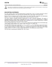
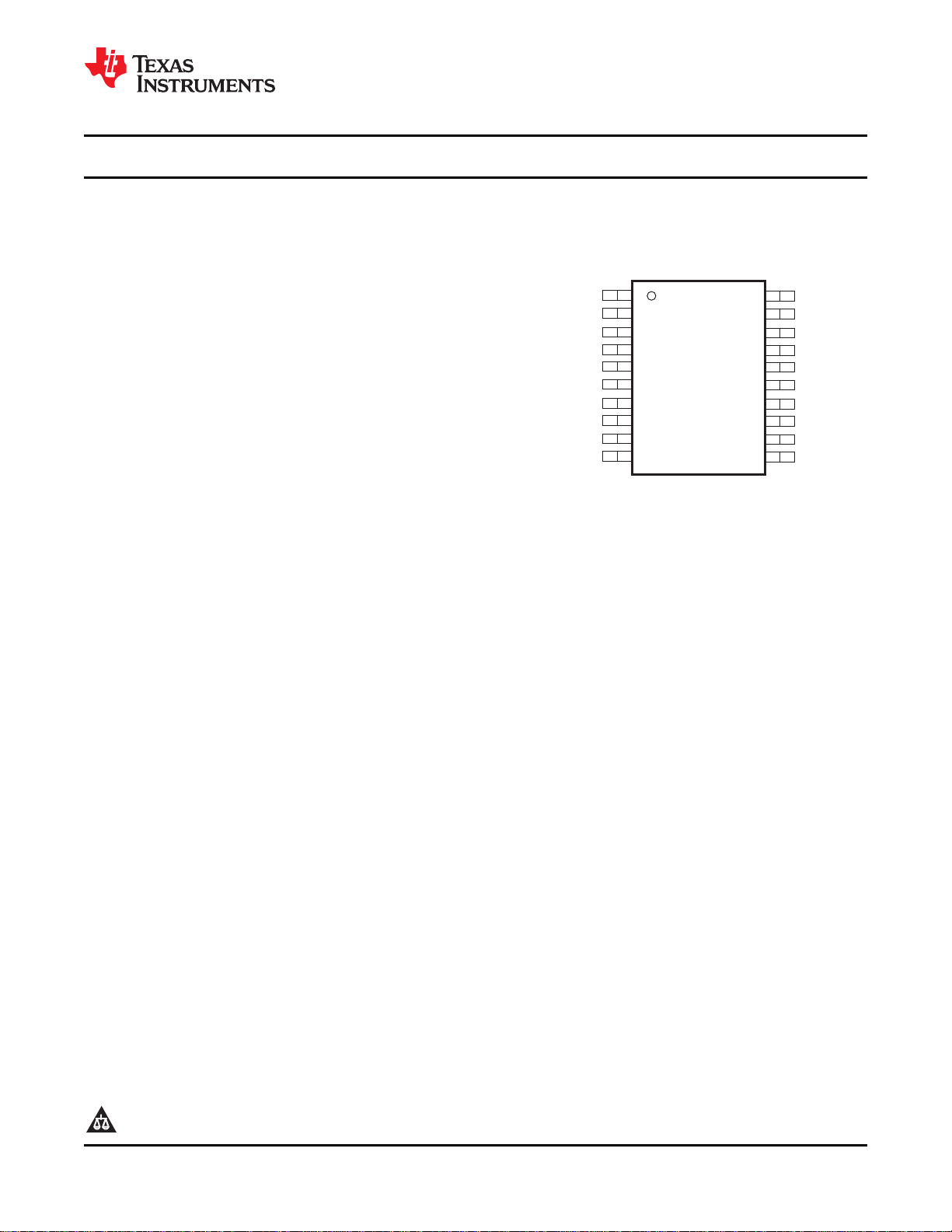
TERMINAL ASSIGNMENT
1
2
3
4
5
6
7
8
9
10
20
19
18
17
16
15
14
13
12
11
S0/A0/CLK_SEL
V
CC
CLK_IN0
CLK_IN1
SCLOCK
Y5
Y4
V
CCOUT2
Y2
V
CCOUT1
Y0
PWPackage
(TopView)
P0087-01
S1/A1
GND
V
CC
GND
SDATA
Y1
GND
Y3
GND
DESCRIPTION
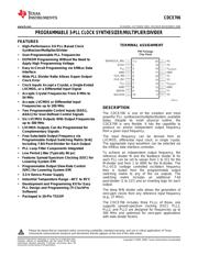
CDCE706
www.ti.com
........................................................................................................................................... SCAS815I – OCTOBER 2005 – REVISED NOVEMBER 2008
PROGRAMMABLE 3-PLL CLOCK SYNTHESIZER/MULTIPLIER/DIVIDER
• High-Performance 3:6 PLL-Based Clock
Synthesizer/Multiplier/Divider
• User-Programmable PLL Frequencies
• EEPROM Programming Without the Need to
Apply High Programming Voltage
• Easy In-Circuit Programming via SMBus Data
Interface
• Wide PLL Divider Ratio Allows 0-ppm Output
Clock Error
• Clock Inputs Accept a Crystal, a Single-Ended
LVCMOS, or a Differential Input Signal
• Accepts Crystal Frequencies From 8 MHz to
54 MHz
• Accepts LVCMOS or Differential Input
Frequencies up to 200 MHz
• Two Programmable Control Inputs [S0/S1,
The CDCE706 is one of the smallest and most
A0/A1] for User-Defined Control Signals
powerful PLL synthesizer/multiplier/dividers available
• Six LVCMOS Outputs With Output Frequencies
today. Despite its small physical outline, the
up to 300 MHz
CDCE706 is very flexible. It has the capability to
produce an almost independent output frequency
• LVCMOS Outputs Can Be Programmed for
from a given input frequency.
Complementary Signals
• Free Selectable Output Frequency via
The input frequency can be derived from an
Programmable Output Switching Matrix [6 × 6]
LVCMOS, differential input clock, or single crystal.
The appropriate input waveform can be selected via
Including 7-Bit Post-Divider for Each Output
the SMBus data interface controller.
• PLL Loop Filter Components Integrated
To achieve an independent output frequency, the
• Low Period Jitter (Typically 60 ps)
reference divider M and the feedback divider N for
• Features Spread-Spectrum Clocking (SSC) for
each PLL can be set to values from 1 to 511 for the
Lowering System EMI
M-divider and from 1 to 4095 for the N-divider. The
• Programmable Output Slew-Rate Control
PLL-VCO (voltage controlled oscillator) frequency
(SRC) for Lowering System EMI
then is routed from the programmable output
switching matrix to any of the six outputs. The
• 3.3-V Device Power Supply
switching matrix includes an additional 7-bit
• Industrial Temperature Range – 40 ° C to 85 ° C
post-divider (1 to 127) and an inverting logic for each
• Development and Programming Kit for Easy
output.
PLL Design and Programming (TI ClockPro
The deep M/N divider ratio allows the generation of
Software)
zero-ppm clocks from any reference input frequency
• Packaged in 20-Pin TSSOP
(e.g., 27 MHz).
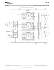
The CDCE706 includes three PLLs; of those, one
supports spread-spectrum clocking (SSC). PLL1,
PLL2, and PLL3 are designed for frequencies up to
300 MHz and optimized for zero-ppm applications
with wide divider factors.
1
Please be aware that an important notice concerning availability, standard warranty, and use in critical applications of Texas
Instruments semiconductor products and disclaimers thereto appears at the end of this data sheet.
PRODUCTION DATA information is current as of publication date.
Copyright © 2005 – 2008, Texas Instruments Incorporated
Products conform to specifications per the terms of the Texas
Instruments standard warranty. Production processing does not
necessarily include testing of all parameters.
器件 Datasheet 文档搜索
AiEMA 数据库涵盖高达 72,405,303 个元件的数据手册,每天更新 5,000 多个 PDF 文件
