Datasheet 搜索 > TI(德州仪器) > CDCP1803-EP 数据手册 > CDCP1803-EP 用户编程技术手册 1/25 页

¥ 0
CDCP1803-EP 用户编程技术手册 - TI(德州仪器)
制造商:
TI(德州仪器)
描述:
具有可编程除法器的增强型产品 1.3 LVPECL 时钟缓冲器
Pictures:
3D模型
符号图
焊盘图
引脚图
产品图
页面导航:
封装尺寸在P18P20P21
标记信息在P18
封装信息在P18P19P20P21
应用领域在P25
导航目录
CDCP1803-EP数据手册
Page:
of 25 Go
若手册格式错乱,请下载阅览PDF原文件
1
FEATURES
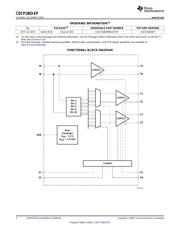
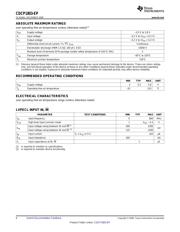
V
SS
(
2)
S0
V
DD
1
Y1
Y1
V
DD
1
V
SS
18
17
16
15
14
13
1
2
3
4
5
6
EN
V
DD
PECL
IN
IN
V
DD
PECL
VBB
24 23 22 21 20 19
7 8 9 10 11 12
S2
V
DD
0
Y0
Y0
V
DD
0
S1
V
SS
V
DD
2
Y2
Y2
V
DD
2
NC
RGE PACKAGE
(TOP VIEW)
(2)
Thermal pad must be connected to V
SS
.
P0024-02
SUPPORTS DEFENSE, AEROSPACE,
DESCRIPTION/ORDERING INFORMATION
CDCP1803-EP
www.ti.com
........................................................................................................................................................................................... SCAS864 – DECEMBER 2008
1:3 LVPECL CLOCK BUFFER WITH PROGRAMMABLE DIVIDER
• Distributes One Differential Clock Input to
Three LVPECL Differential Clock Outputs
• Programmable Output Divider for Two LVPECL
Outputs
• Low-Output Skew 15 ps (Typical)
• V
CC
Range 3 V – 3.6 V
• Signaling Rate Up to 800-MHz LVPECL
• Differential Input Stage for Wide
Common-Mode Range
• Provides VBB Bias Voltage Output for
Single-Ended Input Signals
• Receiver Input Threshold ± 75 mV
• 24-Terminal QFN Package (4 mm × 4 mm)
• Accepts Any Differential Signaling:
LVDS, HSTL, CML, VML, SSTL-2, and
Single-Ended: LVTTL/LVCMOS
AND MEDICAL APPLICATIONS
• Controlled Baseline
• One Assembly/Test Site
• One Fabrication Site
• Available in Military ( – 55 ° C/125 ° C)
Temperature Range
(1)
• Extended Product Life Cycle
• Extended Product-Change Notification
• Product Traceability
(1) Additional temperature ranges available - contact factory
The CDCP1803 clock driver distributes one pair of differential clock inputs to three pairs of LVPECL differential
clock outputs Y[2:0] and Y[2:0] with minimum skew for clock distribution. The CDCP1803 is specifically designed
for driving 50- Ω transmission lines.
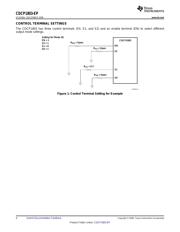
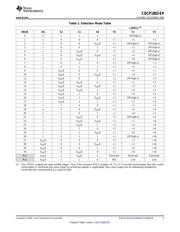
The CDCP1803 has three control terminals, S0, S1, and S2, to select different output mode settings; see Table 1
for details. The CDCP1803 is characterized for operation from – 55 ° C to 125 ° C. For use in single-ended driver
applications, the CDCP1803 also provides a VBB output terminal that can be directly connected to the unused
input as a common-mode voltage reference.
1
Please be aware that an important notice concerning availability, standard warranty, and use in critical applications of Texas
Instruments semiconductor products and disclaimers thereto appears at the end of this data sheet.
PRODUCTION DATA information is current as of publication date.
Copyright © 2008, Texas Instruments Incorporated
Products conform to specifications per the terms of the Texas
Instruments standard warranty. Production processing does not
necessarily include testing of all parameters.
器件 Datasheet 文档搜索
AiEMA 数据库涵盖高达 72,405,303 个元件的数据手册,每天更新 5,000 多个 PDF 文件
