Datasheet 搜索 > 时钟缓冲器、驱动器、锁相环 > Cypress Semiconductor(赛普拉斯) > CY7B991V-5JXIT 数据手册 > CY7B991V-5JXIT 用户编程技术手册 1/21 页
 器件3D模型
¥ 156.878
CY7B991V-5JXIT 用户编程技术手册 - Cypress Semiconductor(赛普拉斯)
制造商:
Cypress Semiconductor(赛普拉斯)
分类:
时钟缓冲器、驱动器、锁相环
封装:
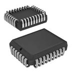
PLCC-32
描述:
CY7B991 系列 8 输出 5 V 100 MHz 可编程偏移时钟缓冲器 表面贴装 - PLCC-32
Pictures:
3D模型
符号图
焊盘图
引脚图
产品图
页面导航:
导航目录
CY7B991V-5JXIT数据手册
Page:
of 21 Go
若手册格式错乱,请下载阅览PDF原文件
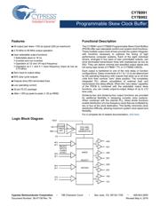
CY7B991
CY7B992
Programmable Skew Clock Buffer
Cypress Semiconductor Corporation • 198 Champion Court • San Jose, CA 95134-1709 • 408-943-2600
Document Number: 38-07138 Rev. *N Revised May 4, 2016
Programmable Skew Clock Buffer
Features
■ All output pair skew <100 ps typical (250 ps maximum)
■ 3.75 MHz to 80 MHz output operation
■ User selectable output functions
❐ Selectable skew to 18 ns
❐ Inverted and non-inverted
❐ Operation at 1⁄2 and 1⁄4 input frequency
❐ Operation at 2 × and 4 × input frequency (input as low as
3.75 MHz)
■ Zero input to output delay
■ 50% duty cycle outputs
■ Outputs drive 50 terminated lines
■ Low operating current
■ 32-pin PLCC package
■ Jitter < 200 ps peak-to-peak (< 25 ps RMS)
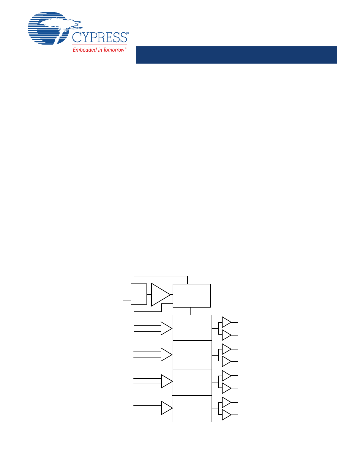
Functional Description
The CY7B991 and CY7B992 Programmable Skew Clock Buffers
(PSCB) offer user selectable control over system clock functions.
These multiple output clock drivers provide the system integrator
with functions necessary to optimize the timing of high
performance computer systems. Each of the eight individual
drivers, arranged in four pairs of user controllable outputs, can
drive terminated transmission lines with impedances as low as
50. They can deliver minimal and specified output skews and
full swing logic levels (CY7B991 TTL or CY7B992 CMOS).
Each output is hardwired to one of the nine delay or function
configurations. Delay increments of 0.7 to 1.5 ns are determined
by the operating frequency with outputs that skew up to ±6 time
units from their nominal “zero” skew position. The completely
integrated PLL allows cancellation of external load and
transmission line delay effects. When this “zero delay” capability
of the PSCB is combined with the selectable output skew
functions, you can create output-to-output delays of up to ±12
time units.
Divide-by-two and divide-by-four output functions are provided
for additional flexibility in designing complex clock systems.
When combined with the internal PLL, these divide functions
enable distribution of a low frequency clock that are multiplied by
two or four at the clock destination. This facility minimizes clock
distribution difficulty, allowing maximum system clock speed and
flexibility.
For a complete list of related documentation, click here.
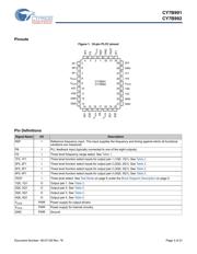
TEST
FB
REF
VCO AND
TIME UNIT
GENERATOR
FS
SELECT
INPUTS
(THREE
LEVEL)
SKEW
SELECT
MATRIX
4F0
4F1
3F0
3F1
2F0
2F1
1F0
1F1
4Q0
4Q1
3Q0
3Q1
2Q0
2Q1
1Q0
1Q1
FILTER
PHASE
FREQ
DET
Logic Block Diagram
器件 Datasheet 文档搜索
AiEMA 数据库涵盖高达 72,405,303 个元件的数据手册,每天更新 5,000 多个 PDF 文件
