Datasheet 搜索 > 微控制器 > Cypress Semiconductor(赛普拉斯) > CY8C21334-24PVXI 数据手册 > CY8C21334-24PVXI 用户编程技术手册 1/55 页
 器件3D模型
¥ 4.739
CY8C21334-24PVXI 用户编程技术手册 - Cypress Semiconductor(赛普拉斯)
制造商:
Cypress Semiconductor(赛普拉斯)
分类:
微控制器
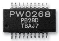
封装:
SSOP-20
描述:
CY8C21 系列 512 B RAM 8 kB 闪存 PSoC® 可编程 片上系统™ - SSOP-20
Pictures:
3D模型
符号图
焊盘图
引脚图
产品图
页面导航:
引脚图在P9P10P11P13P14P15Hot
原理图在P1P4P5
封装尺寸在P34P35P36P37
型号编码规则在P41P42P49
封装信息在P34P41
焊接温度在P38
功能描述在P29P30
技术参数、封装参数在P19P20P21P22P23P24P25P26P27P28P29P30
应用领域在P41
电气规格在P20P26
型号编号列表在P49
导航目录
CY8C21334-24PVXI数据手册
Page:
of 55 Go
若手册格式错乱,请下载阅览PDF原文件
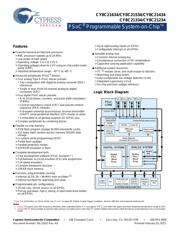
CY8C21634/CY8C21534/CY8C21434
CY8C21334/CY8C21234
PSoC
®
Programmable System-on-Chip™
Cypress Semiconductor Corporation • 198 Champion Court • San Jose, CA 95134-1709 • 408-943-2600
Document Number: 38-12025 Rev. AG Revised February 25, 2015
PSoC
®
Programmable System-on-Chip™
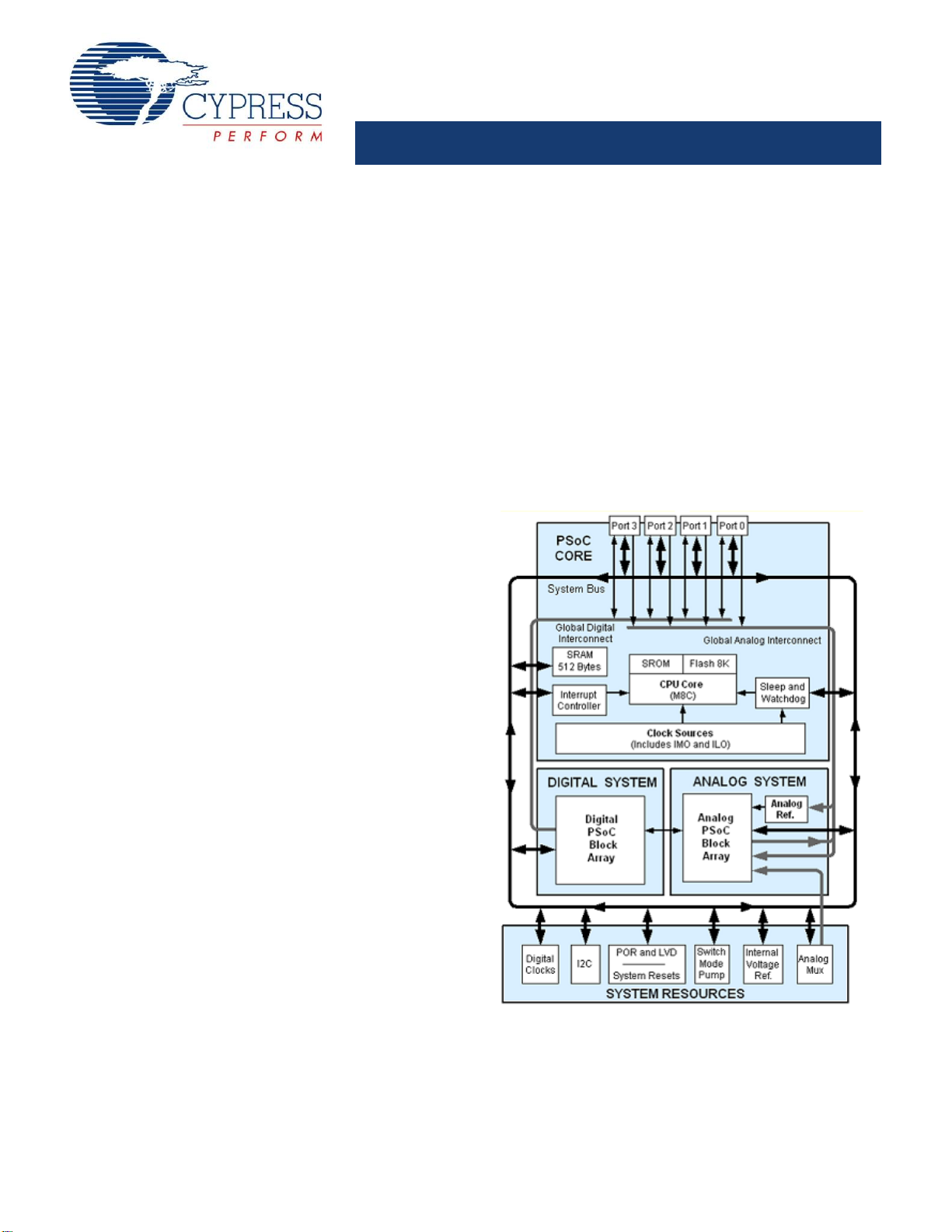
Features
■ Powerful Harvard-architecture processor
❐ M8C processor speeds up to 24 MHz
❐ Low power at high speed
❐ Operating voltage: 2.4 V to 5.25 V
❐ Operating voltages down to 1.0 V using on-chip switch mode
pump (SMP)
❐ Industrial temperature range: –40 °C to +85 °C
■ Advanced peripherals (PSoC
®
blocks)
❐ Four analog Type E PSoC blocks provide:
• Two comparators with digital-to-analog converter (DAC)
references
• Single or dual 10-bit 28 channel analog-to-digital
converters (ADC)
❐ Four digital PSoC blocks provide:
• 8- to 32-bit timers, counters, and pulse width modulators
(PWMs)
• Cyclical redundancy check (CRC) and pseudo random
sequence (PRS) modules
• Full-duplex universal asynchronous receiver transmitter
(UART), serial peripheral interface (SPI) master or slave
• Connectable to all general purpose I/O (GPIO) pins
❐ Complex peripherals by combining blocks
■ Flexible on-chip memory
❐ 8 KB flash program storage 50,000 erase/write cycles
❐ 512 bytes static random access memory (SRAM) data
storage
❐ In-system serial programming (ISSP)
❐ Partial flash updates
❐ Flexible protection modes
❐ EEPROM emulation in flash
■ Complete development tools
❐ Free development software (PSoC Designer™)
❐ Full-featured, in-circuit emulator (ICE) and programmer
❐ Full-speed emulation
❐ Complex breakpoint structure
❐ 128-KB trace memory
■ Precision, programmable clocking
❐ Internal ±2.5% 24- / 48-MHz main oscillator
[1]
❐ Internal oscillator for watchdog and sleep
■ Programmable pin configurations
❐ 25-mA sink, 10-mA source on all GPIOs
❐ Pull-up, pull-down, high Z, strong, or open-drain drive modes
on all GPIOs
❐ Up to eight analog inputs on GPIOs
❐ Configurable interrupt on all GPIOs
■ Versatile analog mux
❐ Common internal analog bus
❐ Simultaneous connection of I/O combinations
❐ Capacitive sensing application capability
■ Additional system resources
❐ I
2
C
[2]
master, slave, and multi-master to 400 kHz
❐ Watchdog and sleep timers
❐ User-configurable low-voltage detection (LVD)
❐ Integrated supervisory circuit
❐ On-chip precision voltage reference
Logic Block Diagram
Errata: For information on silicon errata, see “Errata” on page 49. Details include trigger conditions, devices affected, and proposed workaround.
Notes
1. Errata: The worst case IMO frequency deviation when operated below 0 °C and above +70 °C and within the upper and lower datasheet temperature range is ±5%.
2. Errata:The I
2
C block exhibits occasional data and bus corruption errors when the I
2
C master initiates transactions while the device is transitioning in to or out of sleep
mode.
器件 Datasheet 文档搜索
AiEMA 数据库涵盖高达 72,405,303 个元件的数据手册,每天更新 5,000 多个 PDF 文件
