Datasheet 搜索 > 微控制器 > Microchip(微芯) > DSPIC30F3010-30I/SP 数据手册 > DSPIC30F3010-30I/SP 用户编程技术手册 6/66 页
 器件3D模型
¥ 48.288
DSPIC30F3010-30I/SP 用户编程技术手册 - Microchip(微芯)
制造商:
Microchip(微芯)
分类:
微控制器
封装:
DIP-28
描述:
MICROCHIP DSPIC30F3010-30I/SP 芯片, 数字信号控制器 16位 30MIPS 24K闪存
Pictures:
3D模型
符号图
焊盘图
引脚图
产品图
页面导航:
引脚图在P2Hot
导航目录
DSPIC30F3010-30I/SP数据手册
Page:
of 66 Go
若手册格式错乱,请下载阅览PDF原文件
dsPIC30F Flash Programming Specification
DS70102K-page 6 © 2010 Microchip Technology Inc.
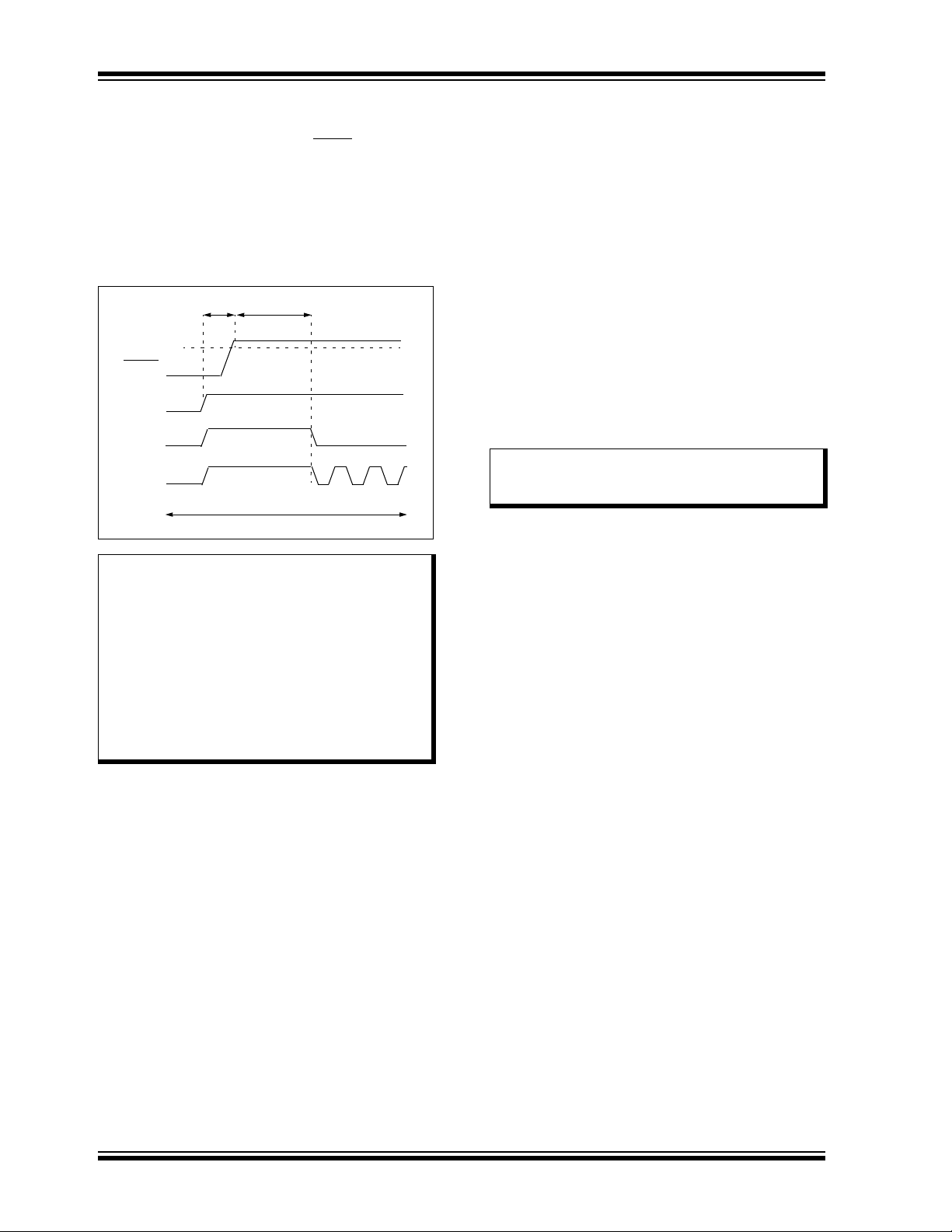
5.2 Entering Enhanced ICSP Mode
The Enhanced ICSP mode is entered by holding PGC
and PGD high, and then raising MCLR/VPP to VIHH
(high voltage), as illustrated in Figure 5-2. In this mode,
the code memory, data EEPROM
and Configuration
bits can be efficiently programmed using the program-
ming executive commands that are serially transferred
using PGC and PGD.
FIGURE 5-2: ENTERING ENHANCED
ICSP™ MODE
5.3 Chip Erase
Before a chip can be programmed, it must be erased.
The Bulk Erase command (ERASEB) is used to perform
this task. Executing this command with the MS
command field set to 0x3 erases all code memory, data
EEPROM and code-protect Configuration bits. The
Chip Erase process sets all bits in these three memory
regions to ‘1’.
Since non-code-protect Configuratio
n bits cannot be
erased, they must be manually set to ‘1’ using multiple
PROGC commands. One PROGC command must be
sent for each Configuration register (see Section 5.7
“Configuration Bits Programming”).
If Advanced Security features are ena
bled, then indi-
vidual Segment Erase operations would need to be
performed, depending on which segment needs to be
programmed at a given stage of system programming.
The user should have the flexibility to select specific
segments for programming.
Note: T
he Device ID registers cannot be erased.
These registers remain intact after a Chip
Erase is performed.
5.4 Blank Check
The term “Blank Check” means to verify that the device
has been successfully erased and has no programmed
memory cells. A blank or erased memory cell reads as
‘1’. The following memories must be blank checked:
• All implemented code memory
•
All implemented data EEPROM
• All Configuration bits (for their default value)
The Device ID registers (0xFF0000:0xFF0002) can be
ig
nored by the Blank Check since this region stores
device information that cannot be erased. Additionally,
all unimplemented memory space should be ignored
from the Blank Check.
The QBLAN
K command is used for the Blank Check. It
determines if the code memory and data EEPROM are
erased by testing these memory regions. A ‘BLANK’ or
‘NOT BLANK’ response is returned. The READD
command is used to read the Configuration registers. If
it is determined that the device is not blank, it must be
erased (see Section 5.3 “Chip Erase”) before
attempting to program the chip.
Note 1: Th
e sequence that places the device into
Enhanced ICSP mode places all unused
I/Os in the high-impedance state.
2: Before entering Enhanced ICSP mode,
clock switching must be disabled using
ICSP, by programming the FCKSM<1:0>
bits in the FOSC Configuration register to
‘11’ or ‘10’.
3: When in Enhanced ICSP mode, the SPI
output pin (SDO1) will toggle while the
device is being programmed.
MCLR/VPP
P7
PGD
PGD = Input
PGC
VDD
VIHH
P6
器件 Datasheet 文档搜索
AiEMA 数据库涵盖高达 72,405,303 个元件的数据手册,每天更新 5,000 多个 PDF 文件
