Datasheet 搜索 > 微控制器 > Microchip(微芯) > DSPIC30F3011-20E/P 数据手册 > DSPIC30F3011-20E/P 用户编程技术手册 2/66 页
 器件3D模型
¥ 50.48
DSPIC30F3011-20E/P 用户编程技术手册 - Microchip(微芯)
制造商:
Microchip(微芯)
分类:
微控制器
封装:
PDIP-40
描述:
PIC 闪存:8K@x24bit RAM:1KB
Pictures:
3D模型
符号图
焊盘图
引脚图
产品图
页面导航:
引脚图在P2Hot
导航目录
DSPIC30F3011-20E/P数据手册
Page:
of 66 Go
若手册格式错乱,请下载阅览PDF原文件
dsPIC30F Flash Programming Specification
DS70102K-page 2 © 2010 Microchip Technology Inc.
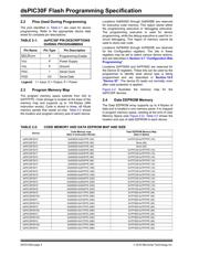
2.2 Pins Used During Programming
The pins identified in Table 2-1 are used for device
programming. Refer to the appropriate device data
sheet for complete pin descriptions.
TABLE 2-1: dsPIC30F PIN DESCRIPTIONS
DURING PROGRAMMING
Pin Name Pin Type Pin Description
MCLR/VPP P Programming Enable
V
DD P Power Supply
VSS P Ground
PGC I Serial Clock
PGD I/O Serial Data
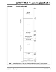
2.3 Program Memory Map
The program memory space extends from 0x0 to
0xFFFFFE. Code storage is located at the base of the
memory map and supports up to 144 Kbytes (48K
instruction wo
rds). Code is stored in three, 48 Kbyte
memory panels that reside on-chip. Table 2-2 shows
the location and program memory size of each device.
Locations 0x800000 through 0x8005BE are reserved
for executive code memory. This region stores either
the programming executive or debugging executive.
The programming executive is used for device
programming, while the debug executive is used for in-
circuit debugging. This region of memory cannot be
used to store user code.
Locations 0xF80000 through 0xF8000E are reserved
fo
r the Configuration registers. The bits in these
registers may be set to select various device options,
and are described in Section 5.7 “Configuration Bits
Programming”.
Locations 0xFF0000 and 0xFF0002 are reserved for
the D
evice ID registers. These bits can be used by the
programmer to identify what device type is being
programmed and are described in Section 10.0
“Device ID”. The device ID reads out normally, even
after code protection is applied.
Figure 2-2 illustrates the memory map for the
dsPIC30F devices.
2.4 Data EEPROM Memory
The Data EEPROM array supports up to 4 Kbytes of
data and is located in one memory panel. It is mapped
in program memory space, residing at the end of User
Memory Space (see Figure 2-2). Ta bl e 2-2 shows the
location and size of dat
a EEPROM in each device.
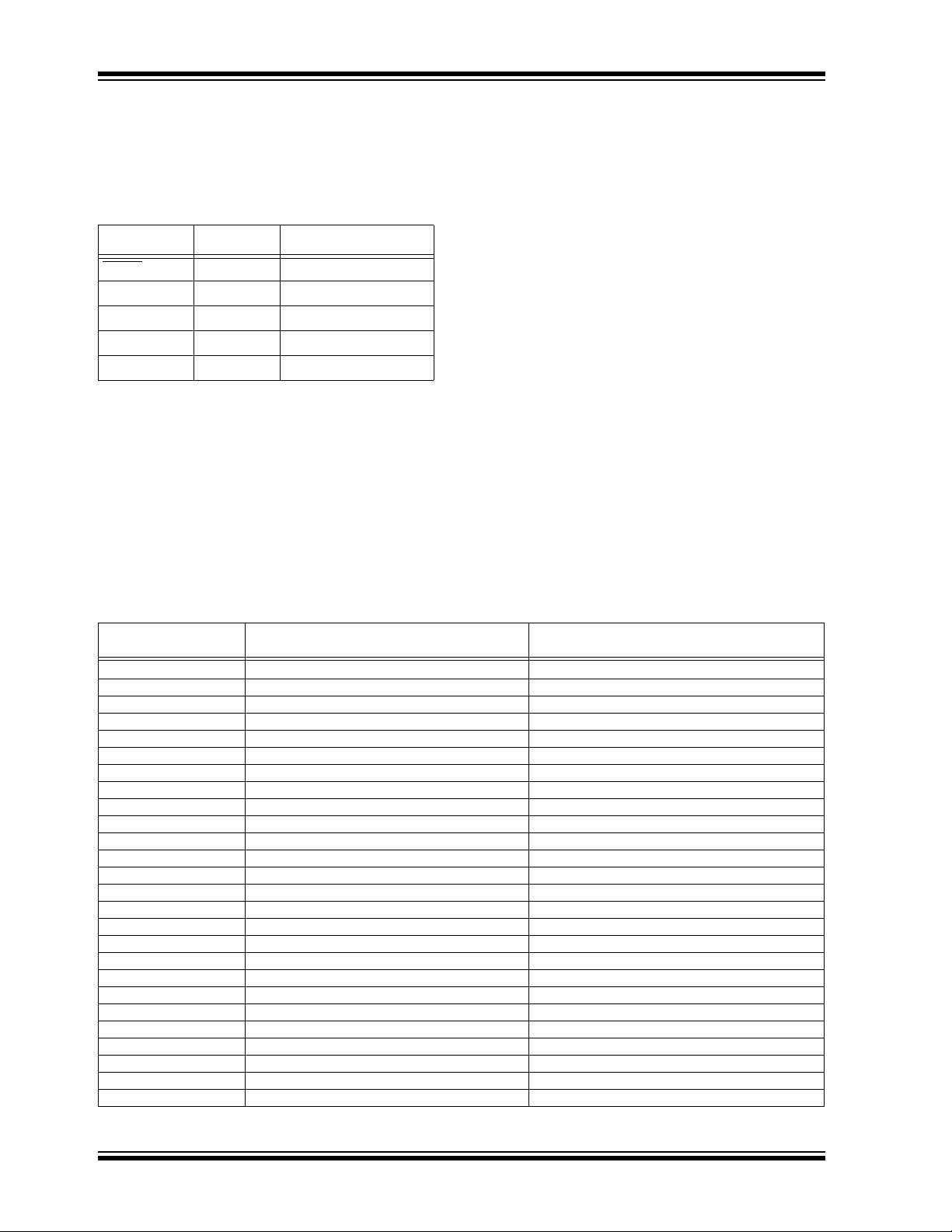
TABLE 2-2: CODE MEMORY AND DATA EEPROM MAP AND SIZE
Device
Code Memory map
(Size in Instruction Words)
Data EEPROM Memory Map
(Size in Bytes)
dsPIC30F2010 0x000000-0x001FFE (4K) 0x7FFC00-0x7FFFFE (1K)
dsPIC30F2011 0x000000-0x001FFE (4K) None (0K)
dsPIC30F2012 0x000000-0x001FFE (4K) None (0K)
dsPIC30F3010 0x000000-0x003FFE (8K) 0x7FFC00-0x7FFFFE (1K)
dsPIC30F3011 0x000000-0x003FFE (8K) 0x7FFC00-0x7FFFFE (1K)
dsPIC30F3012 0x000000-0x003FFE (8K) 0x7FFC00-0x7FFFFE (1K)
dsPIC30F3013 0x000000-0x003FFE (8K) 0x7FFC00-0x7FFFFE (1K)
dsPIC30F3014 0x000000-0x003FFE (8K) 0x7FFC00-0x7FFFFE (1K)
dsPIC30F4011 0x000000-0x007FFE (16K) 0x7FFC00-0x7FFFFE (1K)
dsPIC30F4012 0x000000-0x007FFE (16K) 0x7FFC00-0x7FFFFE (1K)
dsPIC30F4013 0x000000-0x007FFE (16K) 0x7FFC00-0x7FFFFE (1K)
dsPIC30F5011 0x000000-0x00AFFE (22K) 0x7FFC00-0x7FFFFE (1K)
dsPIC30F5013 0x000000-0x00AFFE (22K) 0x7FFC00-0x7FFFFE (1K)
dsPIC30F5015 0x000000-0x00AFFE (22K) 0x7FFC00-0x7FFFFE (1K)
dsPIC30F5016 0x000000-0x00AFFE (22K) 0x7FFC00-0x7FFFFE (1K)
dsPIC30F6010 0x000000-0x017FFE (48K) 0x7FF000-0x7FFFFE (4K)
dsPIC30F6010A 0x000000-0x017FFE (48K) 0x7FF000-0x7FFFFF (4K)
dsPIC30F6011 0x000000-0x015FFE (44K) 0x7FF800-0x7FFFFE (2K)
dsPIC30F6011A 0x000000-0x015FFE (44K) 0x7FF800-0x7FFFFE (2K)
dsPIC30F6012 0x000000-0x017FFE (48K) 0x7FF000-0x7FFFFE (4K)
dsPIC30F6012A 0x000000-0x017FFE (48K) 0x7FF000-0x7FFFFE (4K)
dsPIC30F6013 0x000000-0x015FFE (44K) 0x7FF800-0x7FFFFE (2K)
dsPIC30F6013A 0x000000-0x015FFE (44K) 0x7FF800-0x7FFFFE (2K)
dsPIC30F6014 0x000000-0x017FFE (48K) 0x7FF000-0x7FFFFE (4K)
dsPIC30F6014A 0x000000-0x017FFE (48K) 0x7FF000-0x7FFFFE (4K)
dsPIC30F6015 0x000000-0x017FFE (48K) 0x7FF000-0x7FFFFE (4K)
Legend: I = Input, O = Output, P = Power
器件 Datasheet 文档搜索
AiEMA 数据库涵盖高达 72,405,303 个元件的数据手册,每天更新 5,000 多个 PDF 文件
