Datasheet 搜索 > 微控制器 > Microchip(微芯) > DSPIC33FJ128MC706A-E/PT 数据手册 > DSPIC33FJ128MC706A-E/PT 用户编程技术手册 2/84 页
 器件3D模型
¥ 63.23
DSPIC33FJ128MC706A-E/PT 用户编程技术手册 - Microchip(微芯)
制造商:
Microchip(微芯)
分类:
微控制器
封装:
TQFP-64
描述:
16位 DSC 带128 KB闪存 采用64引脚TQFP封装
Pictures:
3D模型
符号图
焊盘图
引脚图
产品图
页面导航:
引脚图在P2Hot
技术参数、封装参数在P51
电气规格在P59P60
导航目录
DSPIC33FJ128MC706A-E/PT数据手册
Page:
of 84 Go
若手册格式错乱,请下载阅览PDF原文件
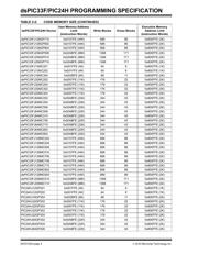
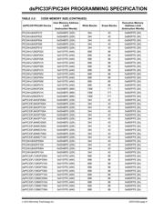
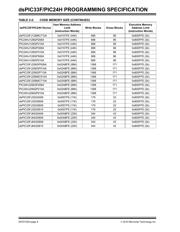
dsPIC33F/PIC24H PROGRAMMING SPECIFICATION
DS70152H-page 2 © 2010 Microchip Technology Inc.
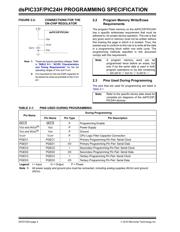
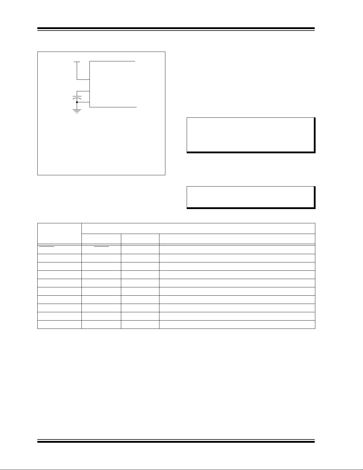
FIGURE 2-2: CONNECTIONS FOR THE
ON-CHIP REGULATOR
2.2 Program Memory Write/Erase
Requirements
The program Flash memory on the dsPIC33F/PIC24H
has a specific write/erase requirement that must be
adhered to, for proper device operation. The rule is that
any given word in memory must not be written without
first erasing the page in which it is located. Thus, the
easiest way to conform to this rule is to write all the data
in a programming block within one write cycle. The
programming methods specified in this document
comply with this requirement.
2.3 Pins Used During Programming
The pins that are used for programming are listed in
Table 2-1.
TABLE 2-1: PINS USED DURING PROGRAMMING
Note 1: These are typical operating voltages. Refer
to TABLE 8-1: “AC/DC Characteristics
and Timing Requirements” for the full
operating ranges of V
DD and VCAP.
2: It is important for the low-ESR capacitor to
be placed as close as possible to the V
CAP
pin.
VDD
VCAP
VSS
dsPIC33F/PIC24H
CEFC
3.3V
Note: A program memory word can be
programmed twice before an erase, but
only if (a) the same data is used in both
program operations or (b) bits containing
‘1’ are set to ‘0’ but no ‘0’ is set to ‘1’.
Note: Refer to the specific device data sheet for
complete pin diagrams of the dsPIC33F/
PIC24H devices.
Pin Name
During Programming
Pin Name Pin Type Pin Description
MCLR MCLR P Programming Enable
V
DD and AVDD
(1)
VDD P Power Supply
VSS and AVSS
(1)
VSS P Ground
V
CAP VCAP P CPU Logic Filter Capacitor Connection
PGEC1 PGEC1 I Primary Programming Pin Pair: Serial Clock
PGED1 PGED1 I/O Primary Programming Pin Pair: Serial Data
PGEC2 PGEC2 I Secondary Programming Pin Pair: Serial Clock
PGED2 PGED2 I/O Secondary Programming Pin Pair: Serial Data
PGEC3 PGEC3 I Tertiary Programming Pin Pair: Serial Clock
PGED3 PGED3 I/O Tertiary Programming Pin Pair: Serial Data
Legend: I = Input O = Output P = Power
Note 1: All power supply and ground pins must be connected, including analog supplies (AV
DD) and ground
(AVSS).
器件 Datasheet 文档搜索
AiEMA 数据库涵盖高达 72,405,303 个元件的数据手册,每天更新 5,000 多个 PDF 文件
