Datasheet 搜索 > 时钟缓冲器、驱动器、锁相环 > Hittite > HMC940LC4B 数据手册 > HMC940LC4B 用户编程技术手册 1/8 页

¥ 2231.356
HMC940LC4B 用户编程技术手册 - Hittite
制造商:
Hittite
分类:
时钟缓冲器、驱动器、锁相环
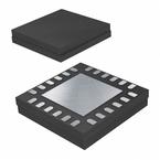
封装:
TFCQFN-24
Pictures:
3D模型
符号图
焊盘图
引脚图
产品图
页面导航:
导航目录
HMC940LC4B数据手册
Page:
of 8 Go
若手册格式错乱,请下载阅览PDF原文件
For price, delivery and to place orders: Hittite Microwave Corporation, 2 Elizabeth Drive, Chelmsford, MA 01824
Phone: 978-250-3343 Fax: 978-250-3373 Order On-line at www.hittite.com
Application Support: Phone: 978-250-3343 or apps@hittite.com
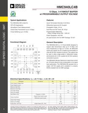
HIGH SPEED DIGITAL LOGIC - SMT
1
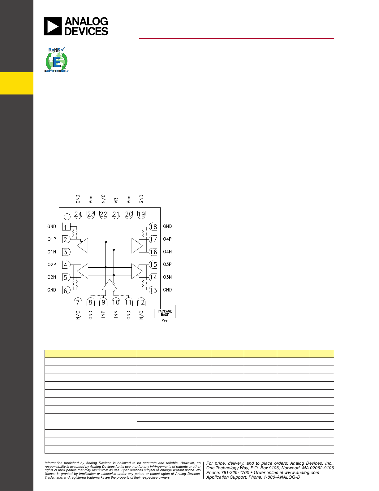
HMC9 40LC4B
v02.0614
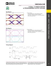
13 Gbps, 1:4 FANOUT BUFFER
w/ PROGRAMMABLE OUTPUT VOLTAGE
The HMC940LC4B is a 1:4 Fanout Buffer designed to
support data transmission rates up to 13 Gbps, and
clock frequencies as high as 13 GHz. All differential
inputs and outputs are DC coupled and terminated on
chip with 50 Ohm resistors to ground. The outputs may
be used in either single-ended or differential modes,
and should be AC or DC coupled into 50 Ohm resistors
connected to ground.
The HMC940LC4B also features an output level control
pin, VR which allows for loss compensation or for signal
level optimization. The HMC940LC4B operates from a
single -3.3V DC supply and is available in a ceramic
RoHS compliant 4x4 mm SMT package.
General Description
Features
Functional Diagram
Inputs Terminated Internally in 50 Ohms
Differential Inputs are DC Coupled
Propagation Delay: 101 ps
Fast Rise and Fall Times: 26 / 25 ps
Programmable Differential
Output Voltage Swing: 600 - 1400 mV
Power Dissipation: 440 mW
24 Lead Ceramic 4x4 mm SMT Package: 16 mm
2
Typical Applications
The HMC940LC4B is ideal for:
• RF ATE Applications
• Broadband Test & Measurement
• Serial Data Transmission up to 13 Gbps
• Clock Buffering up to 13 GHz
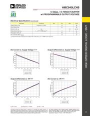
Electrical Specications, T
A
= +25 ºC Vee = -3.3V, VR = 0V
Parameter Conditions Min. Typ. Max Units
Power Supply Voltage (Vee) -3.6 -3.3 -3.0 V
Power Supply Current 133 mA
Maximum Data Rate 13 Gbps
Maximum Clock Rate 13 GHz
Input High Voltage -0.5 0.5 V
Input Low Voltage -1.0 0.0 V
Input Return Loss Frequency <15 GHz 10 dB
Output Amplitude
Single-Ended, peak-to-peak 585 mVp-p
Differential, peak-to-peak 1170 mVp-p
Output High Voltage -15 mV
Output Low Voltage -600 mV
Output Rise / Fall Time Single-Ended, 20% - 80% 26 / 25 ps
Information furnished by Analog Devices is believed to be accurate and reliable. However, no
responsibility is assumed by Analog Devices for its use, nor for any infringements of patents or other
rights of third parties that may result from its use. Specifications subject to change without notice. No
license is granted by implication or otherwise under any patent or patent rights of Analog Devices.
Trademarks and registered trademarks are the property of their respective owners.
For price, delivery, and to place orders: Analog Devices, Inc.,
One Technology Way, P.O. Box 9106, Norwood, MA 02062-9106
Phone: 781-329-4700 • Order online at www.analog.com
Application Support: Phone: 1-800-ANALOG-D
器件 Datasheet 文档搜索
AiEMA 数据库涵盖高达 72,405,303 个元件的数据手册,每天更新 5,000 多个 PDF 文件
