Datasheet 搜索 > FPGA芯片 > Lattice Semiconductor(莱迪思) > ICE40LP1K-CB121 数据手册 > ICE40LP1K-CB121 用户编程技术手册 1/12 页

¥ 33.128
ICE40LP1K-CB121 用户编程技术手册 - Lattice Semiconductor(莱迪思)
制造商:
Lattice Semiconductor(莱迪思)
分类:
FPGA芯片
封装:
BGA-121
描述:
Lattice Semiconductor### 现场可编程门阵列 (FPGA)FPGA 是一种半导体设备,包含通过可编程互连连接的可配置逻辑块 (CLB) 矩阵。 用户通过编程 SRAM 确定这些互连。 CLB 可以简单(与或门等),也可以复杂(RAM 块)。 FPGA 允许对设计进行更改,即使在设备焊接到印刷电路板上之后。
Pictures:
3D模型
符号图
焊盘图
引脚图
产品图
页面导航:
型号编码规则在P2
技术参数、封装参数在P3P5
电气规格在P3P4
导航目录
ICE40LP1K-CB121数据手册
Page:
of 12 Go
若手册格式错乱,请下载阅览PDF原文件
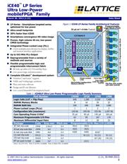
iCE40
™
LP Series
Ultra Low-Power
mobileFPGA
™
Family
March 30, 2012 (1.31)
Data Sheet
© 2007-2012 by Lattice Semiconductor Corporation. All rights reserved. (1.31, 30-MAR-2012)
www.latticesemi.com 1
LP-Series - Smartphone targeted series
optimized for low power
Ultra-small footprints
30% faster than iCE65
Smartphone convergence HD video image
Proven, high-volume 40 nm, low-power
CMOS technology
Integrated Phase-Locked Loop (PLL)
Clock multiplication/division for display, SerDes
and memory interface applications
Up to 533 MHz PLL Output
Reprogrammable from a variety of
methods and sources
Flexible programmable logic and
programmable interconnect fabric
8K look-up tables (LUT4) and flip-flops
Low-power logic and interconnect
Complete iCEcube2
™
development system
Windows
®
and Linux
®
support
VHDL and Verilog logic synthesis
Place and route software
Design and IP core libraries
Low-cost iCEman40LP development board
Table 1:
iCE40LP Ultra Low-Power Programmable Logic Family Summary
Part Number
LP640
LP1K
LP4K
LP8K
Logic Cells (LUT + Flip-Flop)
640
1,280
3,520
7,680
RAM4K Memory Blocks
8
16
20
32
RAM4K RAM bits
32K
64K
80K
128K
Phase-Locked Loops (PLLs)
1
1
2
2
Configuration bits (maximum)
120 Kb
245 Kb
533 Kb
1,057 Kb
Core Operating Power 0 KHz
1
35 µA
40 µA
140 µA
160 µA
Maximum Programmable I/O Pins
63
95
167
178
Maximum Differential Input Pairs
8
12
20
23
Package
Code
Area mm
Pitch mm
Programmable I/O: Max I/O (LVDS)
36
2
-ball chip-scale
BGA
CM36
2.5x2.5
0.4
25(3)
25(3)
49-ball chip-scale BGA
CM49
3x3
0.4
35(5)
35(5)
81-ball chip-scale BGA
CM81
4x4
0.4
63(8)
63(8)
63(9)
3
121-ball chip-scale
BGA
CM121
5x5
0.4
95 (12)
93 (13)
93 (13)
225-ball chip-scale
BGA
CM225
7x7
0.4
167 (20)
178 (23)
84
2
-pin quad no-lead
packall chip-scale BGA
QN84
7x7
0.5
67(7)
Note 1: At 1.2V VCC Note 2: No PLL Available Note 3: Only 1 PLL Available
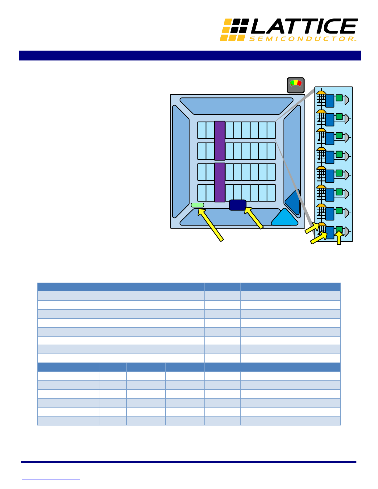
Figure 1:
iCE40 LP-Series Family Architectural Features
I/O Bank 0
I/O Bank 2
I/O Bank 1
I/O Bank 3
PLB
PLB
PLB
PLB
PLB
PLB
PLBPLBPLB
PLBPLBPLB
PLBPLBPLB
Programmable Interconnect
Programmable Interconnect
35 µA at f =0 kHz (Typical)
NVCM
PLBPLBPLB
4Kbit RAM 4Kbit RAM
PLBPLBPLBPLB
Nonvolatile Configuration
Memory (NVCM)
PLBPLBPLBPLB
JTAG
Four-input
Look-Up Table
(LUT4)
Carry logic
Flip-flop with enable
and reset controls
Programmable
Logic Block (PLB)
8 Logic Cells = Programmable Logic Block
PLB
PLB
PLB
PLB
Programmable Interconnect
PLB
PLB
SPI
Config
PLL
Phase-Locked
Loop
器件 Datasheet 文档搜索
AiEMA 数据库涵盖高达 72,405,303 个元件的数据手册,每天更新 5,000 多个 PDF 文件
