Datasheet 搜索 > FPGA芯片 > Lattice Semiconductor(莱迪思) > ICE40LP1K-CB81 数据手册 > ICE40LP1K-CB81 用户编程技术手册 2/12 页

¥ 18.857
ICE40LP1K-CB81 用户编程技术手册 - Lattice Semiconductor(莱迪思)
制造商:
Lattice Semiconductor(莱迪思)
分类:
FPGA芯片
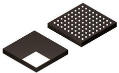
封装:
CSBGA-81
描述:
Lattice Semiconductor### 现场可编程门阵列 (FPGA)FPGA 是一种半导体设备,包含通过可编程互连连接的可配置逻辑块 (CLB) 矩阵。 用户通过编程 SRAM 确定这些互连。 CLB 可以简单(与或门等),也可以复杂(RAM 块)。 FPGA 允许对设计进行更改,即使在设备焊接到印刷电路板上之后。
Pictures:
3D模型
符号图
焊盘图
引脚图
产品图
页面导航:
型号编码规则在P2
技术参数、封装参数在P3P5
电气规格在P3P4
导航目录
ICE40LP1K-CB81数据手册
Page:
of 12 Go
若手册格式错乱,请下载阅览PDF原文件
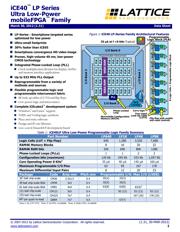
iCE40 LP Series Ultra-Low Power mobileFPGA
™
Family
Lattice Semiconductor Corporation (1.31, 30-MAR-2012)
www.latticesemi.com 2
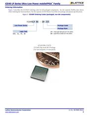
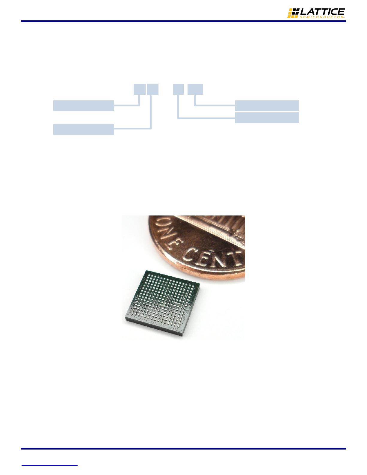
Ordering Information
Figure 2 describes the iCE40LP ordering codes for all packaged components. See the separate DiePlus data sheets
when ordering die-based products. See the separate iCE40 Pinout Excel files for package and pinout specifications.
Figure 2:
iCE40P Ordering Codes (packaged, non-die components)
Low Power Series
Logic Cells
Package Style
iCE40LP 8K - CM 225
Package Leads
CM = chip-scale ball grid (0.4 mm pitch)
QN = quad flat no-lead (0.5 mm pitch)
640, 1K, 4K, 8K
iCE40LP8K-CM225
225-ball Chip-Scale BGA Package
(7x7 mm footprint, 0.4 mm pitch)
器件 Datasheet 文档搜索
AiEMA 数据库涵盖高达 72,405,303 个元件的数据手册,每天更新 5,000 多个 PDF 文件
