Datasheet 搜索 > Central Semiconductor > MC100 数据手册 > MC100 用户编程技术手册 1/17 页


¥ 0
MC100 用户编程技术手册 - Central Semiconductor
制造商:
Central Semiconductor
Pictures:
3D模型
符号图
焊盘图
引脚图
产品图
页面导航:
引脚图在P3Hot
典型应用电路图在P5
原理图在P12
封装尺寸在P16P17
焊盘布局在P17
型号编码规则在P1P15P17
标记信息在P1P15P17
封装信息在P15
技术参数、封装参数在P15
型号编号列表在P7
导航目录
MC100数据手册
Page:
of 17 Go
若手册格式错乱,请下载阅览PDF原文件
© Semiconductor Components Industries, LLC, 2014
June, 2014 − Rev. 2
1 Publication Order Number:
MC100EP195B/D
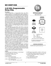
MC100EP195B
3.3V ECL Programmable
Delay Chip
Descriptions
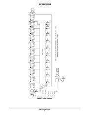
The MC100EP195B is a Programmable Delay Chip (PDC)
designed primarily for clock deskewing and timing adjustment. It
provides variable delay of a differential NECL/PECL input transition.
The delay section consists of a programmable matrix of gates and
multiplexers as shown in the logic diagram, Figure 2. The delay
increment of the EP195B has a digitally selectable resolution of about
10 ps and a net range of up to 10.2 ns. The required delay is selected by
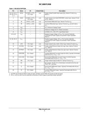
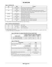
the 10 data select inputs D[9:0] values and controlled by the LEN
(pin 10). A LOW level on LEN allows a transparent LOAD mode of
real time delay values by D[9:0]. A LOW to HIGH transition on LEN
will LOCK and HOLD current values present against any subsequent
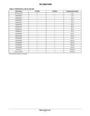
changes in D[10:0]. The approximate delay values for varying tap
numbers correlating to D0 (LSB) through D9 (MSB) are shown in
Table 6 and Figure 3.
The IN/IN
inputs can accept LVPECL (SE of Diff), or LVDS level
signals. Because the EP195B is designed using a chain of multiplexers
it has a fixed minimum delay of 2.2 ns. An additional pin D10 is
provided for controlling Pins 14 and 15, CASCADE and CASCADE
,
also latched by LEN, in cascading multiple PDCs for increased
programmable range. The cascade logic allows full control of multiple
PDCs. Switching devices from all “1” states on D[0:9] with SETMAX
LOW to all “0” states on D[0:9] with SETMAX HIGH will increase
the delay equivalent to “D0”, the minimum increment.
Select input pins D[10:0] may be threshold controlled by
combinations of interconnects between V
EF
(pin 7) and V
CF
(pin 8)
for LVCMOS, ECL, or LVTTL level signals. For LVCMOS input
levels, leave V
CF
and V
EF
open. For ECL operation, short V
CF
and
V
EF
(Pins 7 and 8). For LVTTL level operation, connect a 1.5 V
supply reference to V
CF
and leave open V
EF
pin. The 1.5 V reference
voltage to V
CF
pin can be accomplished by placing a 2.2 kW resistor
between V
CF
and V
EE
for a 3.3 V power supply.
The V
BB
pin, an internally generated voltage supply, is available to
this device only. For single−ended input conditions, the unused
differential input is connected to V
BB
as a switching reference voltage.
V
BB
may also rebias AC coupled inputs. When used, decouple V
BB
and V
CC
via a 0.01 mF capacitor and limit current sourcing or sinking
to 0.5 mA. When not used, V
BB
should be left open.
The 100 Series contains temperature compensation.
Features
• Maximum Input Clock Frequency >1.2 GHz Typical
• Programmable Range: 0 ns to 10 ns
• Delay Range: 2.2 ns to 12.2 ns
• 10 ps Increments
• PECL Mode Operating Range:
V
CC
= 3.0 V to 3.6 V with V
EE
= 0 V
• NECL Mode Operating Range:
V
CC
= 0 V with V
EE
= −3.0 V to −3.6 V
• IN/IN Inputs Accept LVPECL, LVNECL, LVDS Levels
• A Logic High on the EN Pin Will Force Q to Logic Low
• D[10:0] Can Select Either LVPECL, LVCMOS, or
LVTTL Input Levels
• V
BB
Output Reference Voltage
• These are Pb−Free Devices
MARKING
DIAGRAMS*
A = Assembly Location
WL, L = Wafer Lot
Y, YY = Year
W, WW = Work Week
G or G = Pb−Free Package
*For additional marking information, refer to
Application Note AND8002/D.
http://onsemi.com
See detailed ordering and shipping information in the package
dimensions section on page 15 of this data sheet.
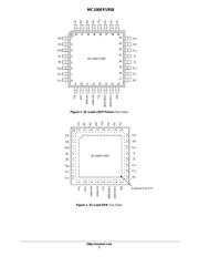
ORDERING INFORMATION
QFN32
MN SUFFIX
CASE 488AM
32
1
MC100
EP195B
ALYWG
G
1
32
1
LQFP−32
FA SUFFIX
CASE 873A
MC100
EP195B
AWLYYWWG
(Note: Microdot may be in either location)
器件 Datasheet 文档搜索
AiEMA 数据库涵盖高达 72,405,303 个元件的数据手册,每天更新 5,000 多个 PDF 文件
