Datasheet 搜索 > ON Semiconductor(安森美) > MC14536B 数据手册 > MC14536B 用户编程技术手册 1/15 页


¥ 0
MC14536B 用户编程技术手册 - ON Semiconductor(安森美)
制造商:
ON Semiconductor(安森美)
描述:
可编程定时器 Programmable Timer
Pictures:
3D模型
符号图
焊盘图
引脚图
产品图
页面导航:
引脚图在P1P5Hot
典型应用电路图在P6P7
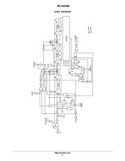
原理图在P2
封装尺寸在P13P14P15
焊盘布局在P13P14
型号编码规则在P1P12P15
标记信息在P1P15
封装信息在P12
技术参数、封装参数在P12
应用领域在P1P12
电气规格在P3
型号编号列表在P1
导航目录
MC14536B数据手册
Page:
of 15 Go
若手册格式错乱,请下载阅览PDF原文件
© Semiconductor Components Industries, LLC, 2014
November, 2014 − Rev. 14
1 Publication Order Number:
MC14536B/D
MC14536B
Programmable Timer
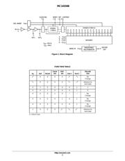
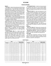
The MC14536B programmable timer is a 24−stage binary ripple
counter with 16 stages selectable by a binary code. Provisions for an
on−chip RC oscillator or an external clock are provided. An on−chip
monostable circuit incorporating a pulse−type output has been
included. By selecting the appropriate counter stage in conjunction
with the appropriate input clock frequency, a variety of timing can be
achieved.
Features
• 24 Flip−Flop Stages − Will Count From 2
0
to 2
24
• Last 16 Stages Selectable By Four−Bit Select Code
• 8−Bypass Input Allows Bypassing of First Eight Stages
• Set and Reset Inputs
• Clock Inhibit and Oscillator Inhibit Inputs
• On−Chip RC Oscillator Provisions
• On−Chip Monostable Output Provisions
• Clock Conditioning Circuit Permits Operation with Very Long Rise
and Fall Times
• Test Mode Allows Fast Test Sequence
• Supply Voltage Range = 3.0 Vdc to 18 Vdc
• Capable of Driving Two Low−Power TTL Loads or One Low−Power
Schottky TTL Load over the Rated Temperature Range
• NLV Prefix for Automotive and Other Applications Requiring
Unique Site and Control Change Requirements; AEC−Q100
Qualified and PPAP Capable
• These Devices are Pb−Free and are RoHS Compliant
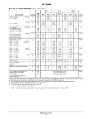
MAXIMUM RATINGS (Voltages Referenced to V
SS
)
Rating
Symbol Value Unit
DC Supply Voltage Range V
DD
−0.5 to +18.0 V
Input or Output Voltage Range
(DC or Transient)
V
in
,
V
out
−0.5 to V
DD
+ 0.5 V
Input or Output Current
(DC or Transient) per Pin
I
in
, I
out
±10 mA
Power Dissipation per Package (Note 1) P
D
500 mW
Ambient Temperature Range T
A
−55 to +125 °C
Storage Temperature Range T
stg
−65 to +150 °C
Lead Temperature, (8−Second Soldering) T
L
260 °C
Stresses exceeding those listed in the Maximum Ratings table may damage the
device. If any of these limits are exceeded, device functionality should not be
assumed, damage may occur and reliability may be affected.
1. Temperature Derating: “D/DW” Packages: –7.0 mW/_C from 65_C to 125_C
This device contains protection circuitry to guard against damage due to high
static voltages or electric fields. However, precautions must be taken to avoid
applications of any voltage higher than maximum rated voltages to this
high−impedance circuit. For proper operation, V
in
and V
out
should be constrained
to the range V
SS
≤ (V
in
or V
out
) ≤ V
DD
.
Unused inputs must always be tied to an appropriate logic voltage level
(e.g., either V
SS
or V
DD
). Unused outputs must be left open.
http://onsemi.com
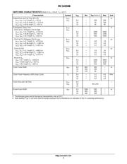
See detailed ordering and shipping information in the package
dimensions section on page 12 of this data sheet.
ORDERING INFORMATION
SOIC−16 WB
DW SUFFIX
CASE 751G
MARKING DIAGRAMS
A = Assembly Location
WL, L = Wafer Lot
YY, Y = Year
WW, W = Work Week
G or G = Pb−Free Package
1
1
14536B
AWLYWWG
SOEIAJ−16
F SUFFIX
CASE 966
MC14536B
ALYWG
1
1
PIN ASSIGNMENT
13
14
15
16
9
10
11
125
4
3
2
1
8
7
6
D
DECODE
OSC INH
MONO−IN
V
DD
A
B
C
OUT 1
IN 1
RESET
SET
V
SS
CLOCK INH
8−BYPASS
OUT 2
SOIC−16 WB
SOEIAJ−16
1
TSSOP−16
DT SUFFIX
CASE 948F
TSSOP−16
14
536B
ALYWG
G
1
16
(Note: Microdot may be in either location)
器件 Datasheet 文档搜索
AiEMA 数据库涵盖高达 72,405,303 个元件的数据手册,每天更新 5,000 多个 PDF 文件
