Datasheet 搜索 > 稳压芯片 > ON Semiconductor(安森美) > MC33269DTRK-5.0G 数据手册 > MC33269DTRK-5.0G 用户编程技术手册 2/17 页

¥ 1.524
MC33269DTRK-5.0G 用户编程技术手册 - ON Semiconductor(安森美)
制造商:
ON Semiconductor(安森美)
分类:
稳压芯片
封装:
TO-252-3
描述:
ON SEMICONDUCTOR MC33269DTRK-5.0G. 芯片, 线性稳压器
Pictures:
3D模型
符号图
焊盘图
引脚图
产品图
页面导航:
引脚图在P1Hot
典型应用电路图在P2
封装尺寸在P16P17
焊盘布局在P16P17
型号编码规则在P1P12P13P17
标记信息在P1P14P15P17
封装信息在P12P13
技术参数、封装参数在P12P13
应用领域在P1P2P9P12P13
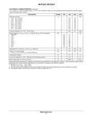
电气规格在P3P4
型号编号列表在P2
导航目录
MC33269DTRK-5.0G数据手册
Page:
of 17 Go
若手册格式错乱,请下载阅览PDF原文件
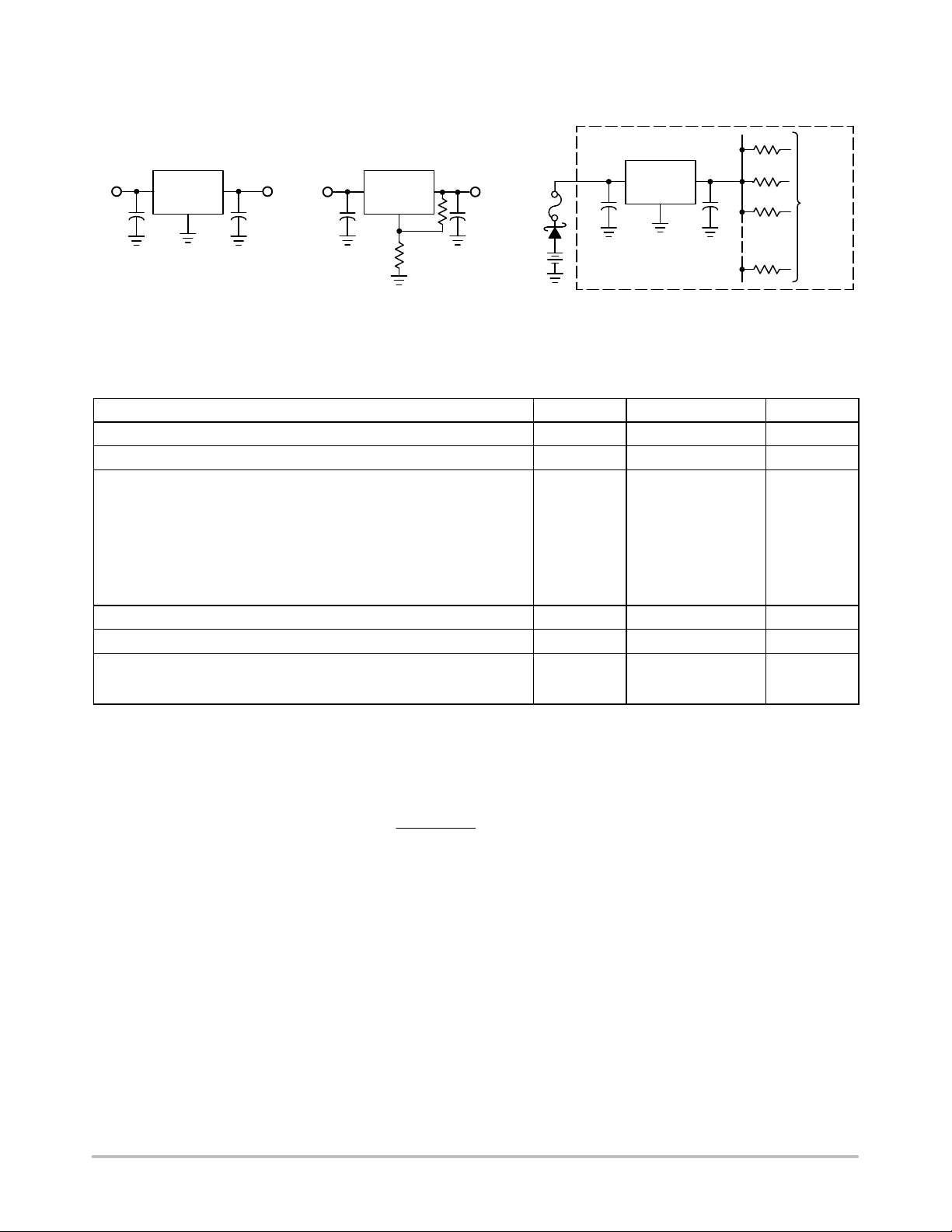
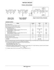
NCP1117, NCV1117
http://onsemi.com
2
10
mF
1
2
Output
10
mF
3
Input
NCP1117
XTXX
++
Figure 1. Fixed
Output Regulator
10
mF
1
2
Output
10
mF
3
Input
NCP1117
XTA
++
Figure 2. Adjustable
Output Regulator
22
mF
1
2
10
mF
3
NCP1117
XT285
++
110 W
110 W
110 W
110 W
4.75 V
to
5.25 V
+
18 to 27
Lines
Figure 3. Active SCSI Bus Terminator
TYPICAL APPLICATIONS
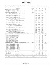
MAXIMUM RATINGS
Rating Symbol Value Unit
Input Voltage (Note 1) V
in
20 V
Output Short Circuit Duration (Notes 2 and 3) − Infinite −
Power Dissipation and Thermal Characteristics
Case 318H (SOT−223)
Power Dissipation (Note 2)
Thermal Resistance, Junction−to−Ambient, Minimum Size Pad
Thermal Resistance, Junction−to−Case
Case 369A (DPAK)
Power Dissipation (Note 2)
Thermal Resistance, Junction−to−Ambient, Minimum Size Pad
Thermal Resistance, Junction−to−Case
P
D
R
q
JA
R
q
JC
P
D
R
q
JA
R
q
JC
Internally Limited
160
15
Internally Limited
67
6.0
W
°C/W
°C/W
W
°C/W
°C/W
Maximum Die Junction Temperature Range T
J
−55 to 150 °C
Storage Temperature Range T
stg
−65 to 150 °C
Operating Ambient Temperature Range
NCP1117
NCV1117
T
A
0 to +125
−40 to +125
°C
Stresses exceeding those listed in the Maximum Ratings table may damage the device. If any of these limits are exceeded, device functionality
should not be assumed, damage may occur and reliability may be affected.
1. This device series contains ESD protection and exceeds the following tests:
Human Body Model (HBM), Class 2, 2000 V
Machine Model (MM), Class B, 200 V
Charge Device Model (CDM), Class IV, 2000 V.
2. Internal thermal shutdown protection limits the die temperature to approximately 175°C. Proper heatsinking is required to prevent activation.
The maximum package power dissipation is:
P
D
+
T
J(max)
* T
A
R
qJA
3. The regulator output current must not exceed 1.0 A with V
in
greater than 12 V.
器件 Datasheet 文档搜索
AiEMA 数据库涵盖高达 72,405,303 个元件的数据手册,每天更新 5,000 多个 PDF 文件
