Datasheet 搜索 > AD转换器 > Microchip(微芯) > MCP3202-BI/P 数据手册 > MCP3202-BI/P 用户编程技术手册 2/34 页
 器件3D模型
¥ 24.748
MCP3202-BI/P 用户编程技术手册 - Microchip(微芯)
制造商:
Microchip(微芯)
分类:
AD转换器
封装:
PDIP-8
描述:
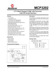
MICROCHIP MCP3202-BI/P 模数转换器, 双路, AEC-Q100, 12 bit, 100 kSPS, 单, 2.7 V, 5.5 V, DIP
Pictures:
3D模型
符号图
焊盘图
引脚图
产品图
页面导航:
导航目录
MCP3202-BI/P数据手册
Page:
of 34 Go
若手册格式错乱,请下载阅览PDF原文件

MCP3202
DS21034F-page 2 1999-2011 Microchip Technology Inc.
1.0 ELECTRICAL
CHARACTERISTICS
Absolute Maximum Ratings †
V
DD
-V
SS
.........................................................................7.0V
All Inputs and Outputs w.r.t. V
SS
............. -0.6V to V
DD
+0.6V
Storage Temperature.....................................-65°C to +150°C
Ambient temperature with power applied.......-65°C to +150°C
Maximum Junction Temperature (T
J
)..........................+150°C
ESD Protection On All Pins (HBM) 4kV
† Notice: Stresses above those listed under “Absolute
Maximum Ratings” may cause permanent damage to the
device. This is a stress rating only and functional operation of
the device at those or any other conditions above those
indicated in the operational listings of this specification is not
implied. Exposure to maximum rating conditions for extended
periods may affect device reliability.
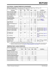
ELECTRICAL CHARACTERISTICS
Electrical Characteristics: Unless otherwise noted, all parameters apply at V
DD
= 5.5V, V
SS
= 0V,
T
A
= -40°C to +85°C, f
SAMPLE
= 100 ksps and f
CLK
= 18*f
SAMPLE
.
Parameter Sym Min. Typ. Max. Units Conditions
Conversion Rate:
Conversion Time t
CONV
— — 12 clock
cycles
Analog Input Sample Time t
SAMPLE
1.5 clock
cycles
Throughput Rate f
SAMPL
—
—
—
—
100
50
ksps
ksps
V
DD
= V
REF
= 5V
V
DD
= V
REF
= 2.7V
DC Accuracy:
Resolution 12 bits
Integral Nonlinearity INL —
—
±0.75
±1
±1
±2
LSB
LSB
MCP3202-B
MCP3202-C
Differential Nonlinearity DNL — ±0.5 ±1 LSB No missing codes over
temperature
Offset Error — ±1.25 ±3 LSB
Gain Error — ±1.25 ±5 LSB
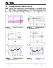
Dynamic Performance:
Total Harmonic Distortion THD — -82 — dB V
IN
= 0.1V to 4.9V@1 kHz
Signal-to-Noise and Distortion
(SINAD)
SINAD — 72 — dB V
IN
= 0.1V to 4.9V@1 kHz
Spurious Free Dynamic Range SFDR — 86 — dB V
IN
= 0.1V to 4.9V@1 kHz
Analog Inputs:
Input Voltage Range for CH0 or
CH1 in Single-Ended Mode
V
SS
—V
DD
V
Input Voltage Range for IN+ in
Pseudo-Differential Mode
IN+ IN- — V
DD
+IN- See Sections 3.1 and 4.1
Input Voltage Range for IN- in
Pseudo-Differential Mode
IN- V
SS
-100 — V
SS
+100 mV See Sections 3.1 and 4.1
Leakage Current — .001 ±1 A
Switch Resistance R
SS
—1k— Ω See Figure 4-1
Sample Capacitor C
SAMPLE
— 20 — pF See Figure 4-1
Digital Input/Output:
Data Coding Format Straight Binary
High Level Input Voltage V
IH
0.7 V
DD
—— V
Low Level Input Voltage V
IL
— — 0.3 V
DD
V
Note 1: This parameter is established by characterization and not 100% tested.
2: Because the sample cap will eventually lose charge, effective clock rates below 10 kHz can affect linearity performance,
especially at elevated temperatures. See Section 6.2 “Maintaining Minimum Clock Speed” for more information.
器件 Datasheet 文档搜索
AiEMA 数据库涵盖高达 72,405,303 个元件的数据手册,每天更新 5,000 多个 PDF 文件
