Datasheet 搜索 > 稳压芯片 > NXP(恩智浦) > MMPF0100F1EPR2 数据手册 > MMPF0100F1EPR2 用户编程技术手册 1/136 页

 器件3D模型
¥ 0
MMPF0100F1EPR2 用户编程技术手册 - NXP(恩智浦)
制造商:
NXP(恩智浦)
分类:
稳压芯片
封装:
QFN-56
描述:
专业电源管理 (PMIC) Power Management IC, i.MX6, pre-prog ,4/6 buck, 6 LDO, 1 boost, QFN 56, Reel
Pictures:
3D模型
符号图
焊盘图
引脚图
产品图
页面导航:
引脚图在P7P8P9P10P22Hot
典型应用电路图在P123P124P125P126P127P128P129
原理图在P6P16P26P41P42P43P54P61P62P63P72P82
封装尺寸在P130
焊盘布局在P128
封装信息在P4P130P131P132P133
功能描述在P15P16P17
技术参数、封装参数在P1P11P13P24P25P27P48P58P69P76P80P81
应用领域在P1P123P124P125P126P127P128P129
电气规格在P13P14P25P27P48P49P50P51P52P58P59P69
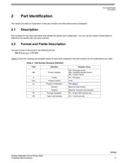
型号编号列表在P5P11
导航目录
MMPF0100F1EPR2数据手册
Page:
of 136 Go
若手册格式错乱,请下载阅览PDF原文件
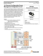
POWER MANAGEMENT
PF0100
Applications
•Tablets
•IPTV
• Industrial control
• Medical monitoring
• Home automation/ alarm/ energy management
EP SUFFIX (E-TYPE)
56 QFN 8X8
98ASA00405D
Consumer and Industrial
Document order number: MMPF0100
Rev. 3.0, 10/2012
Freescale Semiconductor
Advance Information
* This document contains certain information on a new product.
Specifications and information herein are subject to change without notice.
© Freescale Semiconductor, Inc., 2012. All rights reserved.
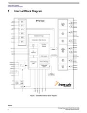
14 Channel Configurable Power
Management Integrated Circuit
The PF0100 Power Management Integrated Circuit (PMIC) provides a
highly programmable/ configurable architecture, with fully integrated
power devices and minimal external components. With up to six buck
converters, six linear regulators, RTC supply, and coin-cell charger,
the PF0100 can provide power for a complete system, including
applications processors, memory, and system peripherals, in a wide
range of applications. With on-chip One Time Programmable (OTP)
memory, the PF0100 is available in pre-programmed standard
versions, or non-programmed to support custom programming. The
PF0100 is especially suited to the I.MX6 family of devices and is
supported by full system level reference designs, and pre-
programmed versions of the device.
Features:
• Four to six buck converters, depending on configuration
• Single/ Dual phase/ parallel options
• DDR termination tracking mode option
• Boost regulator to 5.0 V out
• Six general purpose linear regualtors
• Programmable output voltage, sequence, and timing
• OTP (One Time Programmable) memory for device configuration
• Coin cell charger and RTC supply
• DDR termination reference voltage
• Power control logic with processor interface and event detection
•I
2
C control
• Individually programmable ON, OFF, and Standby modes
VGEN3
100 mA
VGEN5
100 mA
Camera
Audio
Codec
Cluster/HUD
External AMP
Microphones
Speakers
Front USB
POD
Rear USB
POD
Rear Seat
Infotaiment
Sensors
i.MX6X
I
2
C Communication
I
2
C Communication
PF0100
Control Signals
Parallel control/GPIOS
LICELL
Charger
COINCELL
Main Supply
2.8 – 4.5 V
VGEN1
100 mA
VGEN2
250 mA
VGEN4
350 mA
VGEN6
200 mA
SWBST
600 mA
SW3A/B
2500 mA
SW1C
2000 mA
SW1A/B
2500 mA
SW2
2000 mA
SW4
1000 mA
GPS
MIPI
uPCIe
SATA - FLASH
NAND - NOR
Interfaces
Processor Core
Voltages
Camera
VREFDDR
DDR Memory
DDR MEMORY
INTERFACE
SD-MMC/
NAND Mem.
SATA
HDD
WAM
GPS
MIPI
HDMI
LDVS Display
USB
Ethernet
CAN
Figure 1. Simplified Application Diagram
器件 Datasheet 文档搜索
AiEMA 数据库涵盖高达 72,405,303 个元件的数据手册,每天更新 5,000 多个 PDF 文件
