Datasheet 搜索 > 微处理器 > NXP(恩智浦) > MPC8309CVMADDCA 数据手册 > MPC8309CVMADDCA 用户编程技术手册 3/24 页

¥ 240.697
MPC8309CVMADDCA 用户编程技术手册 - NXP(恩智浦)
制造商:
NXP(恩智浦)
分类:
微处理器
封装:
BGA-489
描述:
PowerPC系列 266MHz
Pictures:
3D模型
符号图
焊盘图
引脚图
产品图
MPC8309CVMADDCA数据手册
Page:
of 24 Go
若手册格式错乱,请下载阅览PDF原文件
PROFIBUS on the QUICC Engine Block, Rev. 1
Freescale Semiconductor 3
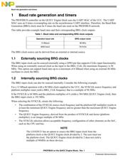
Baud rate generation and timers
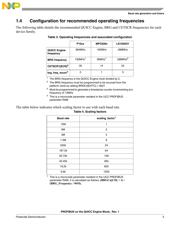
This table details the range of clock and frequency values supported according to the data sheet of each
device.
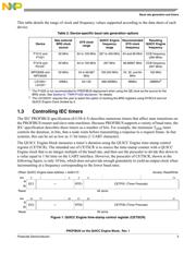
1.3 Controlling IEC timers
The IEC PROFIBUS specification (61158-4-3) describes numerous timers that affect state transitions on
the PROFIBUS master and slave state machines. Because PROFIBUS supports a variety of baud rates, the
IEC specification describes these timers as a number of bits. For example, the minimum T
SDR
timer
controls the duration, in bits, that a node waits before transmitting a response to a request frame. In fast
systems, this can be set as low as 11 bit times (1 UART character).
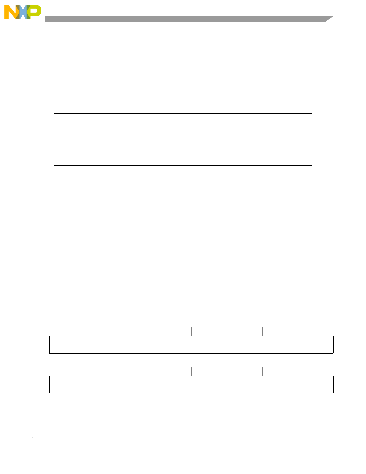
The QUICC Engine block measures a timer’s duration using the QUICC Engine time-stamp control
register (CETSCR). The intended use of CETSCR is to source the time-stamp counter with a QUICC
Engine clock that is an integer multiple of the baud rate, and then use the prescaler to divide this down to
a value equal to 1 bit time on the UART interface. However, the prescaler of CETSCR, shown in the
following figure, is only 10 bits, which does not provide enough granularity to yield an output clock when
incrementing at a frequency corresponding to the lower baud rates.
Table 2. Device-specific baud rate generation options
Device
Max external
BRG clock
source
SYS clock
range
QUICC Engine
frequency
range
Recommended
SYS clock
frequency
Resulting
QUICC Engine
frequency
P1012 and
P1021
50 MHz 64 to 100 MHz 267 to 400 MHz 64 and 96 MHz CCB frequency
(384 MHz)
P1016 and
P0125
1
1
The P1025 is not recommended for PROFIBUS deployment when using the QE clock as the source for the
BRG clock. See Section 6, “TWR-P1025 disclaimer,” for details.
50 MHz 64 to 100 MHz 267 MHz 66.66667 MHz CCB frequency
(267 MHz)
MPC8306 and
MPC8309
50 MHz 24 to 66.667
MHz
150-233 MHz 24, 32, and 64
MHz
192 MHz
LS1020 /
LS1021
50Mhz 64-133 288-300Mhz 96Mhz 288Mhz
2
2
The LS1020/21 requires the user to select the option of clocking the BRG registers using SYSCLK and not
QUICC Engine Clock divided by 2.
Offset QUICC Engine base address + 0x0011C Access: Read/Write
Bits01 456 15
R
EC1 — RTE1 CETPS1 (Timer Prescale)
W
Reset All zeros
Bits 16 17 20 21 22 31
R
EC2 — RTE2 CETPS2 (Timer Prescale)
W
Reset All zeros
Figure 1. QUICC Engine time-stamp control register (CETSCR)
器件 Datasheet 文档搜索
AiEMA 数据库涵盖高达 72,405,303 个元件的数据手册,每天更新 5,000 多个 PDF 文件
