Datasheet 搜索 > 微处理器 > NXP(恩智浦) > MPC8313ECVRAFFC 数据手册 > MPC8313ECVRAFFC 用户编程技术手册 2/28 页
 器件3D模型
¥ 350.673
MPC8313ECVRAFFC 用户编程技术手册 - NXP(恩智浦)
制造商:
NXP(恩智浦)
分类:
微处理器
封装:
PBGA-516
描述:
NXP MPC8313ECVRAFFC 芯片, 微控制器, 32位, POWER, 333MHZ, TEPBGA-II-516
Pictures:
3D模型
符号图
焊盘图
引脚图
产品图
MPC8313ECVRAFFC数据手册
Page:
of 28 Go
若手册格式错乱,请下载阅览PDF原文件

Programming the User-Programmable Machine (UPM) for SDRAM Memory Devices, Rev. 0
2 Freescale Semiconductor
SDRAM Hardware Interfacing
1 SDRAM Hardware Interfacing
An SDRAM’s memory array is divided into two or more banks, which allows one bank to be precharged
while the other is accessed. This is a process known as interleaving and eliminates precharge latency,
which increases bandwidth. Interleaving is not supported on the eLBC, so it cannot be used when
controlling memories through the UPM. Therefore, any access cycles are treated as individual cycles and
the autoprecharge (AP) command is used.
Each SDRAM uses a burst counter to increment column addresses on each clock for burst cycles. The burst
length and burst type (sequential or interleaved) is selected by programming an on-chip mode register. The
user sets the length of the burst sequence to one, two, four, or eight transfers by programming a mode
register of the SDRAM. The burst sequence takes advantage of a three-stage pipeline that allows new
memory accesses to be initiated before the preceding access is complete. If the pipeline is full, data can be
accessed on every clock cycle. After a read burst is complete, the outputs are placed into high impedance
mode until a new access cycle is initiated. Because interleaving is not supported, a sequential burst of
eight transfers should be programmed for a 32-bit bus width.
The internal SDRAM mode register settings determine when to present data-out information during a read
burst. Data can be programmed to appear 1, 2, or 3 clock cycles after a READ command. This feature is
called CAS latency and allows the system designer to delay the data’s appearance onto the bus until the
system is ready. No latencies exist for subsequent cycles in a burst read cycle. While a common CAS
latency is 2, it may vary depending on the device and the considered speed for a specific design.
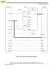
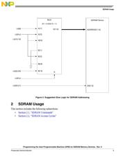
1.1 Hardware Interface
Figure 1 shows the suggested interface from a device using a UPM to an SDRAM. This interface requires
glue logic as described in 1.2, “Address Multiplexing and Bank Select”. The UPM on the device drives
the control, so the CS on the SDRAM is interfaced to one of the LCSn lines on the device, excluding LCS0.
The SDRAM DQM[3:0] signals select the byte lanes and are connected to the appropriate byte strobe
signals (LBS[0:3]) on the device. A10
SD
is connected to LGPL0, which has the functionality to drive an
address either on the line or to a defined level; as a result, A10
SD
acts as both an address line and a control
line. LGPL2 and LGPL3 generate RAS and CAS, and LGPL1 generates WE. LGPL5 drives the address
mux control line, and the device’s LCLK0 signal drives CLK, which is a reference point for the eLBC
controller.
器件 Datasheet 文档搜索
AiEMA 数据库涵盖高达 72,405,303 个元件的数据手册,每天更新 5,000 多个 PDF 文件
