Datasheet 搜索 > 微处理器 > NXP(恩智浦) > MPC885VR66 数据手册 > MPC885VR66 用户编程技术手册 2/12 页

¥ 1627.912
MPC885VR66 用户编程技术手册 - NXP(恩智浦)
制造商:
NXP(恩智浦)
分类:
微处理器
封装:
PBGA-357
Pictures:
3D模型
符号图
焊盘图
引脚图
产品图
MPC885VR66数据手册
Page:
of 12 Go
若手册格式错乱,请下载阅览PDF原文件

MPC885 Family SEC Lite Programming, Rev. 0
2 Freescale Semiconductor
Basics of SEC Lite
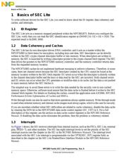
1 Basics of SEC Lite
To write software drivers for the SEC Lite, you need to know about the ID register, data coherency and
caches, and interrupts.
1.1 ID Register
The SEC Lite acts as a memory-mapped peripheral within the MPC885/875. Before you configure the
SEC Lite, verify that you can read the SEC identification register at (IMMR [14–15] = 10) + 1020. The
expected result is 0x2000_0000.
1.2 Data Coherency and Caches
The SEC Lite has its own descriptor-driven DMA controller, and it acts as a master within the
MPC875/885 to fetch items for encryption, including keys and data. SEC descriptors can be directly
written to the SEC crypto-channel descriptor buffer or into memory. When descriptors are written to
memory, the SEC is launched by writing a descriptor pointer to the crypto-channel fetch register. The SEC
then drives the pointers to the MPC875/885 memory controller, and the memory controller returns data
from the requested memory location.
The MPC875/885 caches do not implement hardware snooping to enforce coherency. Therefore, in some
cases, there are channel errors because the SEC descriptor created by the CPU cannot be found at the
memory location written to the SEC fetch register. EU errors occur when the descriptor is directly written
to the channel descriptor buffer and the keys or data read by the SEC are incorrect. Both channel errors
and EU errors can occur when the CPU generates or modifies data in its cache, but the data is not pushed
to main memory before the SEC fetches it.
The simplest way to avoid these errors is to write the data needed by the security core to non-cached
memory space. Otherwise, software must ensure that the data cache is flushed before it writes to the SEC
channel fetch register. For details on flushing the caches, consult the application note AN3066, MPC8XX
Performance Driven Optimization of Caches and MMUs.
Write-through mode can also be used so that store operations always update memory. Write-through mode
is used when external memory and internal cache images must always agree, which is the case for security.
If you are uncertain whether initial SEC difficulties are related to cache coherency, disable the data cache
by clearing the DEN bit in the MPC875/885 data cache control register (DC_CST) to 0. For a full
description of this register, see the section on data cache control registers in the MPC885 Reference
Manual. If disabling the data cache eliminates the problem, then the problem is coherency-related.
1.3 Interrupts
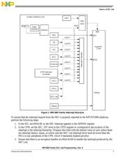
As Figure 1 shows, the SIU receives interrupts from internal sources, such as the FECs, SEC Lite, external
pins, IRQ[0–7], and other modules. The SIU has eight interrupt levels to set the priority of the SIU
interrupt sources (see the chapter on the SIU in the MCP885 Reference Manual). The interrupt level
associated with the SEC Lite interrupt is programmable via the CPTR[SEC_INT] register field, as
described in the chapter on the SEC Lite Master/Slave Interface Module in the MPC885 Reference
Manual.
器件 Datasheet 文档搜索
AiEMA 数据库涵盖高达 72,405,303 个元件的数据手册,每天更新 5,000 多个 PDF 文件
