Datasheet 搜索 > 微处理器 > NXP(恩智浦) > P1022NXN2HFB 数据手册 > P1022NXN2HFB 用户编程技术手册 4/35 页
 器件3D模型
¥ 1557.53
P1022NXN2HFB 用户编程技术手册 - NXP(恩智浦)
制造商:
NXP(恩智浦)
分类:
微处理器
封装:
BBGA-689
描述:
PowerPC系列 1.055GHz
Pictures:
3D模型
符号图
焊盘图
引脚图
产品图


P1022NXN2HFB数据手册
Page:
of 35 Go
若手册格式错乱,请下载阅览PDF原文件
PowerQUICC and QorIQ DDR3 SDRAM Controller Register Setting Considerations, Rev. 4
4 Freescale Semiconductor
Register definitions
2 Register definitions
This section describes the registers and settings discussed in this application note.
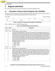
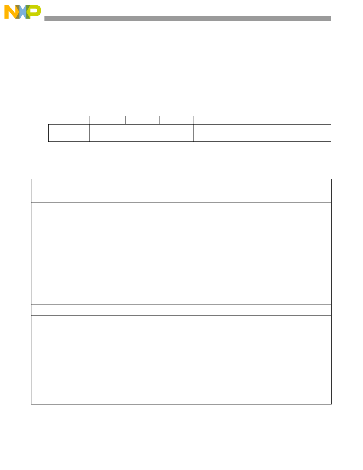
2.1 Chip-Select n Memory Bounds Register (CSn_BOUNDS)
The selections in the chip-select n memory bounds register (CSn_BOUNDS), which is shown in Figure 1,
are based on the size, and starting and ending values of selected memory.
Table 2 describes the CSn_BOUNDS register fields.
Offset 0x000 Access: Read/Write
0 3 4 1516 1920 31
R
—SAn —EAn
W
Figure 1. Chip-Select n Memory Bounds Register (CSn_BOUNDS)
Table 2. CSn_BOUNDS Register field descriptions
Bits Name Description
0–3 — Reserved
4–15 SAn Starting address for chip select (bank) n
This value is compared against the 12 msbs of the 36-bit address.The manufacturer data sheet for the
selected memory should be used to obtain the size of memory. The starting address is usually selected to
be 0x0000_0000_0 for the first chip select (CS0), which is represented by 0 in this field. When there is more
than one chip select, the starting address should consider the CS0 end address to avoid overlapping of
memory space in each chip select. For example, a two-ranked, 2-GB DDR3 DIMM (each rank of 1 GB), can
select the 0 for the starting address of first rank (CS0). The starting address of the second rank (CS1) can
be set to 1 GB at 0x0_4000_0000, which is represented by 0x040 in this field. Another possibility is that the
second rank can start at any location after 1 GB; for example, at 39 GBs at 0x9_C000_0000, which is
represented by 0x9C0 in this field.
Additional examples are as follows:
• 512 MBs --> 0x020
• 1 GB --> 0x040
• 4 GBs --> 0x100
• 8 GBs --> 0x200
16–19 — Reserved
20–31 EAn Ending address for chip select (bank) n
This value is compared against the 12 msbs of the 36-bit address. The end address can be set to the
desired value up to the maximum value of the size of the selected memory. If the end address is set to less
than the “starting address + DRAM size,” it works, but the unassigned memory space remains unused.
For example, a single-rank, 1-GB DDR3 memory DIMM with the starting address of 0 can have the max
ending address of 0x0_3FFF_FFFF to include the entire 1-GB memory space, which is represented by
0x03F in this field. In this example, if a smaller value than 0x03F is selected for the end address, the
unassigned memory space remains unused.
Additional examples are as follows:
• 512 MBs --> 0x01F
• 1 GB --> 0x03F
• 4 GBs --> 0x0FF
• 8 GBs --> 0x1FF
器件 Datasheet 文档搜索
AiEMA 数据库涵盖高达 72,405,303 个元件的数据手册,每天更新 5,000 多个 PDF 文件
