Datasheet 搜索 > 微控制器 > Microchip(微芯) > PIC10F200-E/MC 数据手册 > PIC10F200-E/MC 用户编程技术手册 5/22 页
 器件3D模型
¥ 3.11
PIC10F200-E/MC 用户编程技术手册 - Microchip(微芯)
制造商:
Microchip(微芯)
分类:
微控制器
封装:
DFN-8
描述:
6引脚8位闪存微控制器 6-Pin, 8-Bit Flash Microcontrollers
Pictures:
3D模型
符号图
焊盘图
引脚图
产品图
页面导航:
引脚图在P1Hot
电气规格在P18

导航目录
PIC10F200-E/MC数据手册
Page:
of 22 Go
若手册格式错乱,请下载阅览PDF原文件
2007-2011 Microchip Technology Inc. Advance Information DS41228F-page 5
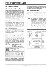
PIC10F200/202/204/206
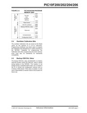
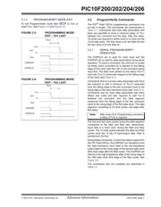
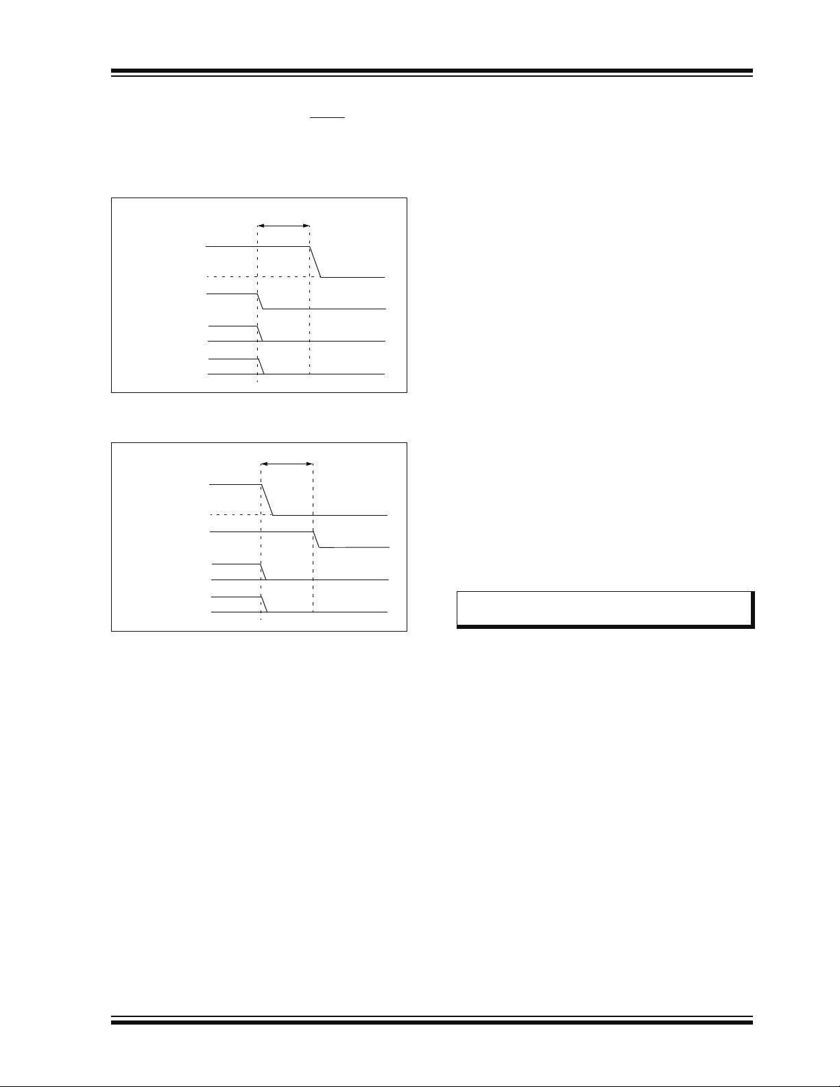
3.1.3 PROGRAM/VERIFY MODE EXIT
To exit Program/Verify mode take MCLR to VDD or
lower (V
IL). See Figure 3-3 and Figure 3-4.
FIGURE 3-3: PROGRAMMING MODE
EXIT – V
PP LAST
FIGURE 3-4: PROGRAMMING MODE
EXIT – V
DD LAST
3.2 Program/Verify Commands
The PIC
®
Flash MCUs programming commands are
six bits in length. The commands are summarized in
Table 3-1. Commands that have data associated with
them are specified to have a minimum delay of T
DLY
between the command and the data. After this delay,
16 clocks are required to either clock in or clock out the
14-bit data word. The first clock is for the Start bit and
the last clock is for the Stop bit.
3.2.1 SERIAL PROGRAM/VERIFY
OPERATION
The ICSPCLK pin is used for clock input and the
ICSPDAT pin is used for data input/output during serial
operation. To input a command, the clock pin is cycled
six times. Each command bit is latched on the falling
edge of the clock with the LSb of the command being
input first. The data must adhere to the setup (T
SET1)
and hold (T
HLD1) times with respect to the falling edge
of the clock (see Table 6-1).
Commands that do not have data associated with them
are required to wait a minimum of T
DLY2 measured
from the falling edge of the last command clock to the
rising edge of the next command clock (see Table 6-1).
Commands that do have data associated with them
(Read and Load) are also required to wait T
DLY2
between the command and the data segment
measured from the falling edge of the last command
clock to the rising edge of the first data clock. The data
segment, consisting of 16 clock cycles, can begin after
this delay.
The first and last clock pulses during the data segment
correspond to the Start and Stop bits, respectively.
Input data is a “don't care” during the Start and Stop
cycles. The 14 clock pulses between the Start and Stop
cycles clock the 14 bits of input/output data. Data is
transferred LSb first.
During Read commands, in which the data is output from
the PIC Flash MCUs, the ICSPDAT pin transitions from
the high-impedance input state to the low-impedance
output state at the rising edge of the second data clock
(first clock edge after the Start cycle). The ICSPDAT pin
returns to the high-impedance state at the rising edge of
the 16th data clock (first edge of the Stop cycle). See
Figure 3-6.
The commands that are available are described in
Table 3-1.
TEXIT
VPP
VDD
ICSPDAT
ICSPCLK
VIHH
VIL
TEXIT
VPP
VDD
ICSPDAT
ICSPCLK
VIHH
VIL
Note: After every End Programming command,
a delay of T
DIS is required.
器件 Datasheet 文档搜索
AiEMA 数据库涵盖高达 72,405,303 个元件的数据手册,每天更新 5,000 多个 PDF 文件
